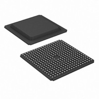
XC3S500E-4FGG320C Xilinx Inc, XC3S500E-4FGG320C Datasheet - Page 125

XC3S500E-4FGG320C
Manufacturer Part Number
XC3S500E-4FGG320C
Description
IC SPARTAN-3E FPGA 500K 320FBGA
Manufacturer
Xilinx Inc
Series
Spartan™-3Er
Datasheet
1.XC3S100E-4VQG100C.pdf
(233 pages)
Specifications of XC3S500E-4FGG320C
Total Ram Bits
368640
Number Of Logic Elements/cells
10476
Number Of Labs/clbs
1164
Number Of I /o
232
Number Of Gates
500000
Voltage - Supply
1.14 V ~ 1.26 V
Mounting Type
Surface Mount
Operating Temperature
0°C ~ 85°C
Package / Case
320-BGA
No. Of Logic Blocks
10476
No. Of Gates
500000
No. Of Macrocells
10476
No. Of Speed Grades
4
No. Of I/o's
250
Clock Management
DLL
Package
320FBGA
Family Name
Spartan®-3E
Device Logic Cells
10476
Device Logic Units
1164
Device System Gates
500000
Number Of Registers
9312
Maximum Internal Frequency
572 MHz
Typical Operating Supply Voltage
1.2 V
Maximum Number Of User I/os
232
Ram Bits
368640
Lead Free Status / RoHS Status
Lead free / RoHS Compliant
For Use With
122-1536 - KIT STARTER SPARTAN-3E
Lead Free Status / RoHS Status
Lead free / RoHS Compliant, Lead free / RoHS Compliant
Other names
122-1526
Available stocks
Company
Part Number
Manufacturer
Quantity
Price
Company:
Part Number:
XC3S500E-4FGG320C
Manufacturer:
XILINX
Quantity:
913
Company:
Part Number:
XC3S500E-4FGG320C
Manufacturer:
XILINX
Quantity:
745
Company:
Part Number:
XC3S500E-4FGG320C
Manufacturer:
Xilinx Inc
Quantity:
10 000
Company:
Part Number:
XC3S500E-4FGG320C
Manufacturer:
XILINX
Quantity:
2 000
Part Number:
XC3S500E-4FGG320C
Manufacturer:
XILINX/赛灵思
Quantity:
20 000
Table 83: DC Characteristics of User I/Os Using Differential Signal Standards
DS312-3 (v3.8) August 26, 2009
Product Specification
Notes:
1.
2.
3.
LVDS_25
BLVDS_25
MINI_LVDS_25
RSDS_25
DIFF_HSTL_I_18
DIFF_HSTL_III_18
DIFF_SSTL18_I
DIFF_SSTL2_I
IOSTANDARD
The numbers in this table are based on the conditions set forth in
Output voltage measurements for all differential standards are made with a termination resistor (R
differential signal pair. The exception is for BLVDS, shown in
At any given time, no more than two of the following differential output standards may be assigned to an I/O bank: LVDS_25, RSDS_25,
MINI_LVDS_25
Attribute
R
Figure 72: External Termination Resistors for BLVDS Transmitter and BLVDS Receiver
(mV)
Min
250
250
300
100
–
–
–
–
Internal
GND level
Logic
V
V
(mV)
V
V
Typ
350
350
OUTN
OUTP
CCO
OD
–
–
–
–
–
–
FPGA
Out
= 2.5V
V
(mV)
Max
OCM
V
V
450
450
600
400
V
–
–
–
–
OD
OH
OL
Figure 71: Differential Output Voltages
50%
= Output common mode voltage =
= Output differential voltage =
= Output voltage indicating a High logic level
= Output voltage indicating a Low logic level
165Ω
165Ω
(mV)
Min
1/4th of Bourns
CAT16-LV4F12
–
–
–
–
–
–
–
–
Part Number
ΔV
V
OCM
OD
(mV)
Max
www.xilinx.com
140Ω
50
–
–
–
–
–
–
–
Figure 72
Table 77
1.125
Min
1.0
1.1
(V)
V
Z
Z
–
–
–
–
–
0
0
V
OUTP
V
below.
= 50Ω
= 50Ω
OD
OUTN
and
V
1.20
Typ
(V)
OCM
–
–
–
–
–
–
–
V
Table
1/4th of Bourns
V
CAT16-PT4F4
OUTP
Part Number
OH
N
P
V
100Ω
OUTP
82.
1.375
- V
Max
(V)
1.4
1.4
–
–
–
–
–
OUTN
Differential
I/O Pair Pins
ds312-3_07_041108
2
+ V
V
FPGA
In
CCO
V
OUTN
OL
(mV)
Min
DC and Switching Characteristics
DS312-3_03_021505
–
–
–
–
–
–
–
–
= 2.5V
T
ΔV
) of 100Ω across the N and P pins of the
OCM
(mV)
Max
50
–
–
–
–
–
–
–
V
V
V
V
CCO
CCO
TT
TT
V
Min
(V)
+ 0.475
+ 0.61
OH
–
–
–
–
– 0.4
– 0.4
V
V
TT
TT
Max
V
(V)
0.4
0.4
– 0.475
– 0.61
–
–
–
–
OL
125


