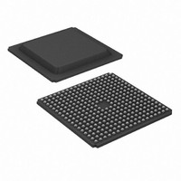
XC3S500E-4FGG320C Xilinx Inc, XC3S500E-4FGG320C Datasheet - Page 24

XC3S500E-4FGG320C
Manufacturer Part Number
XC3S500E-4FGG320C
Description
IC SPARTAN-3E FPGA 500K 320FBGA
Manufacturer
Xilinx Inc
Series
Spartan™-3Er
Datasheet
1.XC3S100E-4VQG100C.pdf
(233 pages)
Specifications of XC3S500E-4FGG320C
Total Ram Bits
368640
Number Of Logic Elements/cells
10476
Number Of Labs/clbs
1164
Number Of I /o
232
Number Of Gates
500000
Voltage - Supply
1.14 V ~ 1.26 V
Mounting Type
Surface Mount
Operating Temperature
0°C ~ 85°C
Package / Case
320-BGA
No. Of Logic Blocks
10476
No. Of Gates
500000
No. Of Macrocells
10476
No. Of Speed Grades
4
No. Of I/o's
250
Clock Management
DLL
Package
320FBGA
Family Name
Spartan®-3E
Device Logic Cells
10476
Device Logic Units
1164
Device System Gates
500000
Number Of Registers
9312
Maximum Internal Frequency
572 MHz
Typical Operating Supply Voltage
1.2 V
Maximum Number Of User I/os
232
Ram Bits
368640
Lead Free Status / RoHS Status
Lead free / RoHS Compliant
For Use With
122-1536 - KIT STARTER SPARTAN-3E
Lead Free Status / RoHS Status
Lead free / RoHS Compliant, Lead free / RoHS Compliant
Other names
122-1526
Available stocks
Company
Part Number
Manufacturer
Quantity
Price
Company:
Part Number:
XC3S500E-4FGG320C
Manufacturer:
XILINX
Quantity:
913
Company:
Part Number:
XC3S500E-4FGG320C
Manufacturer:
XILINX
Quantity:
745
Company:
Part Number:
XC3S500E-4FGG320C
Manufacturer:
Xilinx Inc
Quantity:
10 000
Company:
Part Number:
XC3S500E-4FGG320C
Manufacturer:
XILINX
Quantity:
2 000
Part Number:
XC3S500E-4FGG320C
Manufacturer:
XILINX/赛灵思
Quantity:
20 000
Functional Description
The SLICEM pair supports two additional functions:
•
•
Each of these elements is described in more detail in the fol-
lowing sections.
Logic Cells
The combination of a LUT and a storage element is known
as a “Logic Cell”. The additional features in a slice, such as
the wide multiplexers, carry logic, and arithmetic gates, add
to the capacity of a slice, implementing logic that would oth-
erwise require additional LUTs. Benchmarks have shown
that the overall slice is equivalent to 2.25 simple logic cells.
This calculation provides the equivalent logic cell count
shown in
Slice Details
Figure 15
a superset of the elements and connections to be found in
all slices. The dashed and gray lines (blue when viewed in
color) indicate the resources found only in the SLICEM and
not in the SLICEL.
Each slice has two halves, which are differentiated as top
and bottom to keep them distinct from the upper and lower
slices in a CLB. The control inputs for the clock (CLK), Clock
Table 10: Slice Inputs and Outputs
24
F[4:1]
G[4:1]
BX
BY
BXOUT
BYOUT
ALTDIG
DIG
SLICEWE1
F5
FXINA
FXINB
Fi
CE
SR
Two 16x1 distributed RAM blocks, RAM16
Two 16-bit shift registers, SRL16
Name
Table
is a detailed diagram of the SLICEM. It represents
9.
SLICEL/M Bottom
SLICEL/M Top
SLICEL/M Bottom
SLICEL/M Top
SLICEM Bottom
SLICEM Top
SLICEM Top
SLICEM Top
SLICEM Common
SLICEL/M Bottom
SLICEL/M Top
SLICEL/M Top
SLICEL/M Top
SLICEL/M Common
SLICEL/M Common
Location
Direction
Output
Output
Output
Output
Output
Input
Input
Input
Input
Input
Input
Input
Input
Input
Input
F-LUT and FAND inputs
G-LUT and GAND inputs or Write Address (SLICEM)
Bypass to or output (SLICEM) or storage element, or control input to
F5MUX, input to carry logic, or data input to RAM (SLICEM)
Bypass to or output (SLICEM) or storage element, or control input to
FiMUX, input to carry logic, or data input to RAM (SLICEM)
BX bypass output
BY bypass output
Alternate data input to RAM
ALTDIG or SHIFTIN bypass output
Output from F5MUX; direct feedback to FiMUX
Input to FiMUX; direct feedback from F5MUX or another FiMUX
Input to FiMUX; direct feedback from F5MUX or another FiMUX
Output from FiMUX; direct feedback to another FiMUX
FFX/Y Clock Enable
FFX/Y Set or Reset or RAM Write Enable (SLICEM)
RAM Write Enable
www.xilinx.com
Enable (CE), Slice Write Enable (SLICEWE1), and
Reset/Set (RS) are shared in common between the two
halves.
The LUTs located in the top and bottom portions of the slice
are referred to as "G" and "F", respectively, or the "G-LUT"
and the "F-LUT". The storage elements in the top and bot-
tom portions of the slice are called FFY and FFX, respec-
tively.
Each slice has two multiplexers with F5MUX in the bottom
portion of the slice and FiMUX in the top portion. Depending
on the slice, the FiMUX takes on the name F6MUX,
F7MUX, or F8MUX, according to its position in the multi-
plexer chain. The lower SLICEL and SLICEM both have an
F6MUX. The upper SLICEM has an F7MUX, and the upper
SLICEL has an F8MUX.
The carry chain enters the bottom of the slice as CIN and
exits at the top as COUT. Five multiplexers control the chain:
CYINIT, CY0F, and CYMUXF in the bottom portion and
CY0G and CYMUXG in the top portion. The dedicated arith-
metic logic includes the exclusive-OR gates XORF and
XORG (bottom and top portions of the slice, respectively)
as well as the AND gates FAND and GAND (bottom and top
portions, respectively).
See
put signals.
Table 10
for a description of all the slice input and out-
Description
DS312-2 (v3.8) August 26, 2009
Product Specification
R


