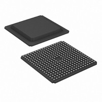
XC3S500E-4FGG320C Xilinx Inc, XC3S500E-4FGG320C Datasheet - Page 164

XC3S500E-4FGG320C
Manufacturer Part Number
XC3S500E-4FGG320C
Description
IC SPARTAN-3E FPGA 500K 320FBGA
Manufacturer
Xilinx Inc
Series
Spartan™-3Er
Datasheet
1.XC3S100E-4VQG100C.pdf
(233 pages)
Specifications of XC3S500E-4FGG320C
Total Ram Bits
368640
Number Of Logic Elements/cells
10476
Number Of Labs/clbs
1164
Number Of I /o
232
Number Of Gates
500000
Voltage - Supply
1.14 V ~ 1.26 V
Mounting Type
Surface Mount
Operating Temperature
0°C ~ 85°C
Package / Case
320-BGA
No. Of Logic Blocks
10476
No. Of Gates
500000
No. Of Macrocells
10476
No. Of Speed Grades
4
No. Of I/o's
250
Clock Management
DLL
Package
320FBGA
Family Name
Spartan®-3E
Device Logic Cells
10476
Device Logic Units
1164
Device System Gates
500000
Number Of Registers
9312
Maximum Internal Frequency
572 MHz
Typical Operating Supply Voltage
1.2 V
Maximum Number Of User I/os
232
Ram Bits
368640
Lead Free Status / RoHS Status
Lead free / RoHS Compliant
For Use With
122-1536 - KIT STARTER SPARTAN-3E
Lead Free Status / RoHS Status
Lead free / RoHS Compliant, Lead free / RoHS Compliant
Other names
122-1526
Available stocks
Company
Part Number
Manufacturer
Quantity
Price
Company:
Part Number:
XC3S500E-4FGG320C
Manufacturer:
XILINX
Quantity:
913
Company:
Part Number:
XC3S500E-4FGG320C
Manufacturer:
XILINX
Quantity:
745
Company:
Part Number:
XC3S500E-4FGG320C
Manufacturer:
Xilinx Inc
Quantity:
10 000
Company:
Part Number:
XC3S500E-4FGG320C
Manufacturer:
XILINX
Quantity:
2 000
Part Number:
XC3S500E-4FGG320C
Manufacturer:
XILINX/赛灵思
Quantity:
20 000
Pinout Descriptions
Table 124: Types of Pins on Spartan-3E FPGAs (Continued)
Differential Pair Labeling
I/Os with Lxxy_# are part of a differential pair. ‘L’ indicates
differential capability. The “xx” field is a two-digit integer,
unique to each bank that identifies a differential pin-pair.
The ‘y’ field is either ‘P’ for the true signal or ‘N’ for the
inverted signal in the differential pair. The ‘#’ field is the I/O
bank number.
The pin name suffix has the following significance.
Figure 80
input to and a differential output from Bank 1.
164
Notes:
1.
2.
Color Code
VCCAUX
CONFIG
VCCINT
VCCO
Type /
# = I/O bank number, an integer between 0 and 3.
IRDY/TRDY designations are for PCI designs; refer to PCI documentation for details.
JTAG
GND
N.C.
provides a specific example showing a differential
Dedicated configuration pin. Not available as a user-I/O pin. Every package
has two dedicated configuration pins. These pins are powered by
VCCAUX. See the
Dedicated JTAG pin. Not available as a user-I/O pin. Every package has
four dedicated JTAG pins. These pins are powered by VCCAUX.
Dedicated ground pin. The number of GND pins depends on the package
used. All must be connected.
Dedicated auxiliary power supply pin. The number of VCCAUX pins
depends on the package used. All must be connected to +2.5V. See the
Powering Spartan-3E FPGAs
Dedicated internal core logic power supply pin. The number of VCCINT
pins depends on the package used. All must be connected to +1.2V. See
the
Along with all the other VCCO pins in the same bank, this pin supplies
power to the output buffers within the I/O bank and sets the input threshold
voltage for some I/O standards. See the
section in Module 2 for details.
This package pin is not connected in this specific device/package
combination but may be connected in larger devices in the same package.
Powering Spartan-3E FPGAs
Spartan-3E
Bank 0
FPGA
Bank 2
Configuration
Figure 80: Differential Pair Labeling
Description
section in Module 2 for details.
section in Module 2 for details.
section in Module 2 for details.
www.xilinx.com
Powering Spartan-3E FPGAs
"xx" is a two-digit integer, unique for each bank, that
identifies a differential pin-pair.
‘y’ is replaced by ‘P’ for the true signal or ‘N’ for the
inverted. These two pins form one differential pin-pair.
‘#’ is an integer, 0 through 3, indicating the associated
I/O bank.
‘L’ indicates that the pin is part of a differential pair.
IO_L38P_1
IO_L38N_1
IO_L39P_1
IO_L39N_1
Pair Number
Positive Polarity
True Receiver
Negative Polarity
Inverted Receiver
Bank Number
DONE, PROG_B
TDI, TMS, TCK, TDO
GND
VCCAUX
VCCINT
VCCO_#
N.C.
DS312-4_00_032409
DS312-4 (v3.8) August 26, 2009
Pin Name(s) in Type
Product Specification
R


