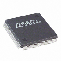
EPF8452AQC160-4 Altera, EPF8452AQC160-4 Datasheet - Page 34

EPF8452AQC160-4
Manufacturer Part Number
EPF8452AQC160-4
Description
IC FLEX 8000A FPGA 4K 160-PQFP
Manufacturer
Altera
Series
FLEX 8000r
Datasheet
1.EPF8282ATC100-3.pdf
(62 pages)
Specifications of EPF8452AQC160-4
Number Of Logic Elements/cells
336
Number Of Labs/clbs
42
Number Of I /o
120
Number Of Gates
4000
Voltage - Supply
4.75 V ~ 5.25 V
Mounting Type
Surface Mount
Operating Temperature
0°C ~ 85°C
Package / Case
160-MQFP, 160-PQFP
Lead Free Status / RoHS Status
Contains lead / RoHS non-compliant
Total Ram Bits
-
Other names
544-2259
Available stocks
Company
Part Number
Manufacturer
Quantity
Price
Company:
Part Number:
EPF8452AQC160-4
Manufacturer:
GENESIS
Quantity:
569
Part Number:
EPF8452AQC160-4
Manufacturer:
ALTERA/阿尔特拉
Quantity:
20 000
FLEX 8000 Programmable Logic Device Family Data Sheet
34
Notes to tables:
(1)
(2)
(3)
(4)
(5)
(6)
(7)
t
t
t
t
t
t
t
t
t
t
Table 20. FLEX 8000 External Reference Timing Characteristics
ODH
Table 19. FLEX 8000 Interconnect Timing Parameters
LABCASC
LABCARRY
LOCAL
ROW
COL
DIN_C
DIN_D
DIN_IO
DRR
Internal timing parameters cannot be measured explicitly. They are worst-case delays based on testable and
external parameters specified by Altera. Internal timing parameters should be used for estimating device
performance. Post-compilation timing simulation or timing analysis is required to determine actual worst-case
performance.
These values are specified in
For the t
The t
timing analysis is required to determine actual worst-case performance.
External reference timing characteristics are factory-tested, worst-case values specified by Altera. A representative
subset of signal paths is tested to approximate typical device applications.
For more information on test conditions, see
This parameter is a guideline that is sample-tested only and is based on extensive device characterization. This
parameter applies to global and non-global clocking, and for LE and I/O element registers.
Symbol
Symbol
ROW
OD3
and t
f
and t
DIN_D
Register-to-register delay via 4 LEs, 3 row interconnects, and 4 local interconnects
Output data hold time after clock
Cascade delay between LEs in different LABs
Carry delay between LEs in different LABs
LAB local interconnect delay
Row interconnect routing delay
Column interconnect routing delay
Dedicated input to LE control delay
Dedicated input to LE data delay (4)
Dedicated input to IOE control delay
ZX3
parameters, V
delays are worst-case values for typical applications. Post-compilation timing simulation or
The FLEX 8000 timing model shows the delays for various paths and
functions in the circuit. See
parts: the LE; the IOE; and the interconnect, including the row and column
FastTrack Interconnect, LAB local interconnect, and carry and cascade
interconnect paths. Each parameter shown in
worst-case value in
FLEX 8000 timing model and these timing parameters can be used to
estimate FLEX 8000 device performance. Timing simulation or timing
analysis after compilation is required to determine the final worst-case
performance.
Figure
For more information on timing parameters, go to
(Understanding FLEX 8000
Table 10 on page 28
19.
CCIO
= 3.3 V or 5.0 V.
Table 21
Application Note 76 (Understanding FLEX 8000
or
(4)
Tables 22
(7)
Table 14 on page
summarizes the interconnect paths shown in
Timing).
Parameter
Parameter
Figure
Note (1)
through 49. Hand-calculations that use the
19. This model contains three distinct
29.
Note (5)
Figure 19
Application Note 76
Timing).
Altera Corporation
is expressed as a
(6)


