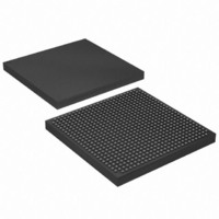
EP1S20F672I7 Altera, EP1S20F672I7 Datasheet - Page 205

EP1S20F672I7
Manufacturer Part Number
EP1S20F672I7
Description
IC STRATIX FPGA 20K LE 672-FBGA
Manufacturer
Altera
Series
Stratix®r
Datasheet
1.EP1S10F780C7.pdf
(276 pages)
Specifications of EP1S20F672I7
Number Of Logic Elements/cells
18460
Number Of Labs/clbs
1846
Total Ram Bits
1669248
Number Of I /o
426
Voltage - Supply
1.425 V ~ 1.575 V
Mounting Type
Surface Mount
Operating Temperature
-40°C ~ 100°C
Package / Case
672-FBGA
Family Name
Stratix
Number Of Logic Blocks/elements
18460
# I/os (max)
426
Frequency (max)
420.17MHz
Process Technology
0.13um (CMOS)
Operating Supply Voltage (typ)
1.5V
Logic Cells
18460
Ram Bits
1669248
Operating Supply Voltage (min)
1.425V
Operating Supply Voltage (max)
1.575V
Operating Temp Range
-40C to 100C
Operating Temperature Classification
Industrial
Mounting
Surface Mount
Pin Count
672
Package Type
FBGA
Lead Free Status / RoHS Status
Contains lead / RoHS non-compliant
Number Of Gates
-
Lead Free Status / Rohs Status
Not Compliant
Available stocks
Company
Part Number
Manufacturer
Quantity
Price
Part Number:
EP1S20F672I7
Manufacturer:
ALTERA/阿尔特拉
Quantity:
20 000
Company:
Part Number:
EP1S20F672I7N
Manufacturer:
ALTERA20
Quantity:
212
Altera Corporation
January 2006
Table 4–54
clock networks.
Notes to
(1)
(2)
Notes to
(1)
(2)
t
t
t
t
t
t
t
t
t
t
XZPLL
ZXPLL
INSU
INH
OUTCO
INSUPLL
INHPLL
OUTCOPLL
XZPLL
ZXPLL
Table 4–53. Stratix Regional Clock External I/O Timing Parameters (Part 2
of 2)
Table 4–54. Stratix Global Clock External I/O Timing Parameters
(2)
Symbol
Symbol
These timing parameters are sample-tested only.
These timing parameters are for column and row IOE pins. You should use the
Quartus II software to verify the external timing for any pin.
These timing parameters are sample-tested only.
These timing parameters are for column and row IOE pins. You should use the
Quartus II software to verify the external timing for any pin.
Notes
Table
Table
shows the external I/O timing parameters when using global
Setup time for input or bidirectional pin using IOE input register with
global clock fed by
Hold time for input or bidirectional pin using IOE input register with
global clock fed by
Clock-to-output delay output or bidirectional pin using IOE output
register with global clock fed by
Setup time for input or bidirectional pin using IOE input register with
global clock fed by Enhanced PLL with default phase setting
Hold time for input or bidirectional pin using IOE input register with
global clock fed by Enhanced PLL with default phase setting
Clock-to-output delay output or bidirectional pin using IOE output
register with global clock Enhanced PLL with default phase setting
Synchronous IOE output enable register to output pin disable delay
using global clock fed by Enhanced PLL with default phase setting
Synchronous IOE output enable register to output pin enable delay
using global clock fed by Enhanced PLL with default phase setting
Synchronous IOE output enable register to output pin disable delay
using regional clock fed by Enhanced PLL with default phase setting
Synchronous IOE output enable register to output pin enable delay
using regional clock fed by Enhanced PLL with default phase setting
(1),
4–53:
4–54:
(2)
CLK
CLK
pin
pin
Parameter
Parameter
Stratix Device Handbook, Volume 1
CLK
DC & Switching Characteristics
pin
Notes
(1),
4–35


