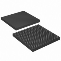
EP1S20F672I7 Altera, EP1S20F672I7 Datasheet - Page 267

EP1S20F672I7
Manufacturer Part Number
EP1S20F672I7
Description
IC STRATIX FPGA 20K LE 672-FBGA
Manufacturer
Altera
Series
Stratix®r
Datasheet
1.EP1S10F780C7.pdf
(276 pages)
Specifications of EP1S20F672I7
Number Of Logic Elements/cells
18460
Number Of Labs/clbs
1846
Total Ram Bits
1669248
Number Of I /o
426
Voltage - Supply
1.425 V ~ 1.575 V
Mounting Type
Surface Mount
Operating Temperature
-40°C ~ 100°C
Package / Case
672-FBGA
Family Name
Stratix
Number Of Logic Blocks/elements
18460
# I/os (max)
426
Frequency (max)
420.17MHz
Process Technology
0.13um (CMOS)
Operating Supply Voltage (typ)
1.5V
Logic Cells
18460
Ram Bits
1669248
Operating Supply Voltage (min)
1.425V
Operating Supply Voltage (max)
1.575V
Operating Temp Range
-40C to 100C
Operating Temperature Classification
Industrial
Mounting
Surface Mount
Pin Count
672
Package Type
FBGA
Lead Free Status / RoHS Status
Contains lead / RoHS non-compliant
Number Of Gates
-
Lead Free Status / Rohs Status
Not Compliant
Available stocks
Company
Part Number
Manufacturer
Quantity
Price
Part Number:
EP1S20F672I7
Manufacturer:
ALTERA/阿尔特拉
Quantity:
20 000
Company:
Part Number:
EP1S20F672I7N
Manufacturer:
ALTERA20
Quantity:
212
- Current page: 267 of 276
- Download datasheet (4Mb)
Altera Corporation
January 2006
t
t
t
t
t
t
t
f
t
t
f
% spread
t
f
f
f
f
t
OUTDUTY
JITTER
CONFIG5,6
CONFIG11,12
SCANCLK
DLOCK
LOCK
VCO
LSKEW
SKEW
SS
ARESET
IN
INPFD
INDUTY
EINDUTY
INJITTER
Table 4–129. Enhanced PLL Specifications for -7 Speed Grade (Part 2 of 2)
Table 4–130. Enhanced PLL Specifications for -8 Speed Grade (Part 1 of 3)
Symbol
Symbol
Duty cycle for external clock output
(when set to 50%)
Period jitter for external clock output
(6)
Time required to reconfigure the
scan chains for PLLs 5 and 6
Time required to reconfigure the
scan chains for PLLs 11 and 12
scanclk frequency
Time required to lock dynamically
(after switchover or reconfiguring any
non-post-scale counters/delays)
(11)
Time required to lock from end of
device configuration
PLL internal VCO operating range
Clock skew between two external
clock outputs driven by the same
counter
Clock skew between two external
clock outputs driven by the different
counters with the same settings
Spread spectrum modulation
frequency
Percentage spread for spread
spectrum frequency
Minimum pulse width on
signal
Input clock frequency
Input frequency to PFD
Input clock duty cycle
External feedback clock input duty
cycle
Input clock period jitter
Parameter
Parameter
(10)
(5)
(11)
areset
(7)
(1),
Min
Min
300
0.5
(9)
40
40
45
10
30
10
3
3
(2)
Typ
±50
±75
Typ
±20 mUI for <200-MHz outclk
±100 ps for >200-MHz outclk
Stratix Device Handbook, Volume 1
DC & Switching Characteristics
289/f
193/f
±200
600
Max
480
420
Max
100
400
150
60
60
0.6
55
22
SCANCLK
SCANCLK
(8)
(3)
MHz
MHz
Unit
ps or
MHz
MHz
Unit
mUI
kHz
ps
%
%
ps
ps
ns
μs
μs
%
%
4–97
Related parts for EP1S20F672I7
Image
Part Number
Description
Manufacturer
Datasheet
Request
R

Part Number:
Description:
CYCLONE II STARTER KIT EP2C20N
Manufacturer:
Altera
Datasheet:

Part Number:
Description:
CPLD, EP610 Family, ECMOS Process, 300 Gates, 16 Macro Cells, 16 Reg., 16 User I/Os, 5V Supply, 35 Speed Grade, 24DIP
Manufacturer:
Altera Corporation
Datasheet:

Part Number:
Description:
CPLD, EP610 Family, ECMOS Process, 300 Gates, 16 Macro Cells, 16 Reg., 16 User I/Os, 5V Supply, 15 Speed Grade, 24DIP
Manufacturer:
Altera Corporation
Datasheet:

Part Number:
Description:
Manufacturer:
Altera Corporation
Datasheet:

Part Number:
Description:
CPLD, EP610 Family, ECMOS Process, 300 Gates, 16 Macro Cells, 16 Reg., 16 User I/Os, 5V Supply, 30 Speed Grade, 24DIP
Manufacturer:
Altera Corporation
Datasheet:

Part Number:
Description:
High-performance, low-power erasable programmable logic devices with 8 macrocells, 10ns
Manufacturer:
Altera Corporation
Datasheet:

Part Number:
Description:
High-performance, low-power erasable programmable logic devices with 8 macrocells, 7ns
Manufacturer:
Altera Corporation
Datasheet:

Part Number:
Description:
Classic EPLD
Manufacturer:
Altera Corporation
Datasheet:

Part Number:
Description:
High-performance, low-power erasable programmable logic devices with 8 macrocells, 10ns
Manufacturer:
Altera Corporation
Datasheet:

Part Number:
Description:
Manufacturer:
Altera Corporation
Datasheet:

Part Number:
Description:
Manufacturer:
Altera Corporation
Datasheet:

Part Number:
Description:
Manufacturer:
Altera Corporation
Datasheet:

Part Number:
Description:
CPLD, EP610 Family, ECMOS Process, 300 Gates, 16 Macro Cells, 16 Reg., 16 User I/Os, 5V Supply, 25 Speed Grade, 24DIP
Manufacturer:
Altera Corporation
Datasheet:


