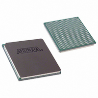
EP1S30F780I6N Altera, EP1S30F780I6N Datasheet - Page 110

EP1S30F780I6N
Manufacturer Part Number
EP1S30F780I6N
Description
IC STRATIX FPGA 30K LE 780-FBGA
Manufacturer
Altera
Series
Stratix®r
Datasheet
1.EP1S10F780C7.pdf
(276 pages)
Specifications of EP1S30F780I6N
Number Of Logic Elements/cells
32470
Number Of Labs/clbs
3247
Total Ram Bits
3317184
Number Of I /o
597
Voltage - Supply
1.425 V ~ 1.575 V
Mounting Type
Surface Mount
Operating Temperature
-40°C ~ 100°C
Package / Case
780-FBGA
Lead Free Status / RoHS Status
Lead free / RoHS Compliant
Number Of Gates
-
Available stocks
Company
Part Number
Manufacturer
Quantity
Price
Company:
Part Number:
EP1S30F780I6N
Manufacturer:
ALTERA
Quantity:
996
- Current page: 110 of 276
- Download datasheet (4Mb)
PLLs & Clock Networks
2–96
Stratix Device Handbook, Volume 1
Clock Feedback
The following four feedback modes in Stratix device enhanced PLLs
allow multiplication and/or phase and delay shifting:
■
■
■
■
Phase & Delay Shifting
Stratix device enhanced PLLs provide advanced programmable phase
and clock delay shifting. These parameters are set in the Quartus II
software.
Phase Delay
The Quartus II software automatically sets the phase taps and counter
settings according to the phase shift entry. You enter a desired phase shift
and the Quartus II software automatically sets the closest setting
achievable. This type of phase shift is not reconfigurable during system
operation. For phase shifting, enter a phase shift (in degrees or time units)
for each PLL clock output port or for all outputs together in one shift. You
can select phase-shifting values in time units with a resolution of 156.25
to 416.66 ps. This resolution is a function of frequency input and the
multiplication and division factors (that is, it is a function of the VCO
period), with the finest step being equal to an eighth (×0.125) of the VCO
period. Each clock output counter can choose a different phase of the
Zero delay buffer: The external clock output pin is phase-aligned
with the clock input pin for zero delay. Altera recommends using the
same I/O standard on the input clock and the output clocks for
optimum performance.
External feedback: The external feedback input pin, FBIN, is phase-
aligned with the clock input, CLK, pin. Aligning these clocks allows
you to remove clock delay and skew between devices. This mode is
only possible for PLLs 5 and 6. PLLs 5 and 6 each support feedback
for one of the dedicated external outputs, either one single-ended or
one differential pair. In this mode, one e counter feeds back to the PLL
FBIN input, becoming part of the feedback loop. Altera recommends
using the same I/O standard on the input clock, the FBIN pin, and
the output clocks for optimum performance.
Normal mode: If an internal clock is used in this mode, it is phase-
aligned to the input clock pin. The external clock output pin will
have a phase delay relative to the clock input pin if connected in this
mode. You define which internal clock output from the PLL should
be phase-aligned to the internal clock pin.
No compensation: In this mode, the PLL will not compensate for any
clock networks or external clock outputs.
Altera Corporation
July 2005
Related parts for EP1S30F780I6N
Image
Part Number
Description
Manufacturer
Datasheet
Request
R

Part Number:
Description:
CYCLONE II STARTER KIT EP2C20N
Manufacturer:
Altera
Datasheet:

Part Number:
Description:
CPLD, EP610 Family, ECMOS Process, 300 Gates, 16 Macro Cells, 16 Reg., 16 User I/Os, 5V Supply, 35 Speed Grade, 24DIP
Manufacturer:
Altera Corporation
Datasheet:

Part Number:
Description:
CPLD, EP610 Family, ECMOS Process, 300 Gates, 16 Macro Cells, 16 Reg., 16 User I/Os, 5V Supply, 15 Speed Grade, 24DIP
Manufacturer:
Altera Corporation
Datasheet:

Part Number:
Description:
Manufacturer:
Altera Corporation
Datasheet:

Part Number:
Description:
CPLD, EP610 Family, ECMOS Process, 300 Gates, 16 Macro Cells, 16 Reg., 16 User I/Os, 5V Supply, 30 Speed Grade, 24DIP
Manufacturer:
Altera Corporation
Datasheet:

Part Number:
Description:
High-performance, low-power erasable programmable logic devices with 8 macrocells, 10ns
Manufacturer:
Altera Corporation
Datasheet:

Part Number:
Description:
High-performance, low-power erasable programmable logic devices with 8 macrocells, 7ns
Manufacturer:
Altera Corporation
Datasheet:

Part Number:
Description:
Classic EPLD
Manufacturer:
Altera Corporation
Datasheet:

Part Number:
Description:
High-performance, low-power erasable programmable logic devices with 8 macrocells, 10ns
Manufacturer:
Altera Corporation
Datasheet:

Part Number:
Description:
Manufacturer:
Altera Corporation
Datasheet:

Part Number:
Description:
Manufacturer:
Altera Corporation
Datasheet:

Part Number:
Description:
Manufacturer:
Altera Corporation
Datasheet:

Part Number:
Description:
CPLD, EP610 Family, ECMOS Process, 300 Gates, 16 Macro Cells, 16 Reg., 16 User I/Os, 5V Supply, 25 Speed Grade, 24DIP
Manufacturer:
Altera Corporation
Datasheet:


