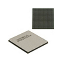
EP4SGX530HH35C2N Altera, EP4SGX530HH35C2N Datasheet - Page 17

EP4SGX530HH35C2N
Manufacturer Part Number
EP4SGX530HH35C2N
Description
IC STRATIX IV FPGA 530K 1152HBGA
Manufacturer
Altera
Series
Stratix® IV GXr
Datasheets
1.EP4SGX110DF29C3N.pdf
(80 pages)
2.EP4SGX110DF29C3N.pdf
(1154 pages)
3.EP4SGX110DF29C3N.pdf
(432 pages)
4.EP4SGX110DF29C3N.pdf
(22 pages)
5.EP4SGX110DF29C3N.pdf
(30 pages)
6.EP4SGX110DF29C3N.pdf
(72 pages)
7.EP4SGX530HH35C2N.pdf
(1145 pages)
Specifications of EP4SGX530HH35C2N
Number Of Logic Elements/cells
531200
Number Of Labs/clbs
21248
Total Ram Bits
27376
Number Of I /o
564
Voltage - Supply
0.87 V ~ 0.93 V
Mounting Type
Surface Mount
Operating Temperature
0°C ~ 85°C
Package / Case
1152-HBGA
Family Name
Stratix® IV
Number Of Logic Blocks/elements
531200
# Registers
424960
# I/os (max)
560
Process Technology
40nm
Operating Supply Voltage (typ)
900mV
Logic Cells
531200
Ram Bits
28033024
Operating Supply Voltage (min)
0.87V
Operating Supply Voltage (max)
0.93V
Operating Temp Range
0C to 85C
Operating Temperature Classification
Commercial
Mounting
Surface Mount
Pin Count
1152
Package Type
FCHBGA
Lead Free Status / RoHS Status
Lead free / RoHS Compliant
Number Of Gates
-
Lead Free Status / Rohs Status
Compliant
Available stocks
Company
Part Number
Manufacturer
Quantity
Price
Chapter 1: DC and Switching Characteristics for Stratix IV Devices
Electrical Characteristics
Table 1–13. Pin Capacitance for Stratix IV Devices
April 2011 Altera Corporation
C
C
C
C
C
C
and C
IOTB
IOLR
CLKTB
CLKLR
OUTFB
CLK1
, C
CLK10
Symbol
CLK3
, C
CLK8
,
Table 1–12
Table 1–12. OCT Variation after Power-Up Calibration
Pin Capacitance
Table 1–13
Hot Socketing
Table 1–14
Table 1–14. Hot Socketing Specifications for Stratix IV Devices
Input capacitance on the top and bottom I/O pins
Input capacitance on the left and right I/O pins
Input capacitance on the top and bottom non-dedicated clock input pins
Input capacitance on the left and right non-dedicated clock input pins
Input capacitance on the dual-purpose clock output and feedback pins
Input capacitance for dedicated clock input pins
dR/dV
dR/dT
Note to
(1) Valid for V
I
I
I
I
Notes to
(1) The I/O ramp rate is 10 ns or more. For ramp rates faster than 10 ns, |I
(2) These specifications are preliminary.
IOPIN (DC)
IOPIN (AC)
XC VR- TX ( DC)
XC VR- RX ( DC)
Symbol
capacitance and dv/dt is the slew rate.
Symbol
Table
Table
(2)
(2)
lists the OCT variation after the power-up calibration.
lists the Stratix IV device family pin capacitance.
lists the hot socketing specifications for Stratix IV devices.
1–12:
CCIO
1–14:
OCT variation with voltage without
re-calibration
OCT variation with temperature
without re-calibration
range of ±5% and temperature range of 0° to 85°C.
DC current per I/O pin
AC current per I/O pin
DC current per transceiver TX pin
DC current per transceiver RX pin
Description
Description
Description
Stratix IV Device Handbook Volume 4: Device Datasheet and Addendum
(Note 1)
V
CCIO
3.0
2.5
1.8
1.5
1.2
3.0
2.5
1.8
1.5
1.2
(V)
IOPIN
| = C dv/dt, in which C is the I/O pin
0.0297
0.0344
0.0499
0.0744
0.1241
Typical
0.189
0.208
0.266
0.273
0.317
Value
Maximum
8 mA
100 mA
300 μA
50 mA
4
4
4
4
5
2
(1)
%/mV
%/°C
Unit
Unit
pF
pF
pF
pF
pF
pF
1–9


