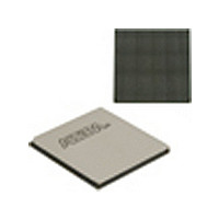
EP4SGX530HH35C2N Altera, EP4SGX530HH35C2N Datasheet - Page 49

EP4SGX530HH35C2N
Manufacturer Part Number
EP4SGX530HH35C2N
Description
IC STRATIX IV FPGA 530K 1152HBGA
Manufacturer
Altera
Series
Stratix® IV GXr
Datasheets
1.EP4SGX110DF29C3N.pdf
(80 pages)
2.EP4SGX110DF29C3N.pdf
(1154 pages)
3.EP4SGX110DF29C3N.pdf
(432 pages)
4.EP4SGX110DF29C3N.pdf
(22 pages)
5.EP4SGX110DF29C3N.pdf
(30 pages)
6.EP4SGX110DF29C3N.pdf
(72 pages)
7.EP4SGX530HH35C2N.pdf
(1145 pages)
Specifications of EP4SGX530HH35C2N
Number Of Logic Elements/cells
531200
Number Of Labs/clbs
21248
Total Ram Bits
27376
Number Of I /o
564
Voltage - Supply
0.87 V ~ 0.93 V
Mounting Type
Surface Mount
Operating Temperature
0°C ~ 85°C
Package / Case
1152-HBGA
Family Name
Stratix® IV
Number Of Logic Blocks/elements
531200
# Registers
424960
# I/os (max)
560
Process Technology
40nm
Operating Supply Voltage (typ)
900mV
Logic Cells
531200
Ram Bits
28033024
Operating Supply Voltage (min)
0.87V
Operating Supply Voltage (max)
0.93V
Operating Temp Range
0C to 85C
Operating Temperature Classification
Commercial
Mounting
Surface Mount
Pin Count
1152
Package Type
FCHBGA
Lead Free Status / RoHS Status
Lead free / RoHS Compliant
Number Of Gates
-
Lead Free Status / Rohs Status
Compliant
Available stocks
Company
Part Number
Manufacturer
Quantity
Price
Chapter 1: DC and Switching Characteristics for Stratix IV Devices
Switching Characteristics
Table 1–30. Transceiver Block Jitter Specifications for Stratix IV GX Devices
April 2011 Altera Corporation
Sinusoidal Jitter tolerance at
1536 Mbps
Sinusoidal Jitter tolerance at
3072 Mbps
Notes to
(1) Dedicated refclk pins were used to drive the input reference clocks.
(2) The Jitter numbers are valid for the stated conditions only.
(3) The jitter numbers for SONET/SDH are compliant to the GR-253-CORE Issue 3 Specification.
(4) The jitter numbers for Fibre Channel are compliant to the FC-PI-4 Specification revision 6.10.
(5) The jitter numbers for XAUI are compliant to the IEEE802.3ae-2002 Specification.
(6) The jitter numbers for PCI Express (PIPE) (PCIe) are compliant to the PCIe Base Specification 2.0.
(7) The jitter numbers for Serial RapidIO are compliant to the RapidIO Specification 1.3.
(8) The jitter numbers for GIGE are compliant to the IEEE802.3-2002 Specification.
(9) The jitter numbers for HiGig are compliant to the IEEE802.3ae-2002 Specification.
(10) The jitter numbers for (OIF) CEI are compliant to the OIF-CEI-02.0 Specification.
(11) The HD-SDI and 3G-SDI jitter numbers are compliant to the SMPTE292M and SMPTE424M Specifications.
(12) The fibre channel transmitter jitter generation numbers are compliant to the specification at δ
(13) The fibre channel receiver jitter tolerance numbers are compliant to the specification at δ
(14) You must use the ATX PLL adjacent to the transceiver channels to meet the transmitter jitter generation compliance in PCIe Gen2 ×8 modes.
(15) Stratix IV PCIe receivers are compliant to this specification provided the V
(16) The jitter numbers for Serial Attached SCSI (SAS) are compliant to the SAS-2.1 Specification.
(17) The jitter numbers for CPRI are compliant to the CPRI Specification V3.0.
(18) The jitter numbers for OBSAI are compliant to the OBSAI RP3 Specification V4.1.
Table
Description
Symbol/
1–30:
Jitter Frequency =
10.9 KHz
Pattern = CJPAT
Jitter Frequency =
921.6 MHz to 20 MHz
Pattern = CJPAT
Jitter Frequency = 21.8
KHz
Pattern = CJPAT
Jitter Frequency =
1843.2 MHz to 20 MHz
Pattern = CJPAT
Conditions
Min
–2 Commercial
Speed Grade
Stratix IV Device Handbook Volume 4: Device Datasheet and Addendum
Typ
> 8.5
> 0.1
> 8.5
> 0.1
TX-CM-DC-ACTIVEIDLE-DELTA
Max
R
interoperability point.
Min
(Note
–2× Commercial
–3 Commercial/
T
Industrial and
Speed Grade
interoperability point.
of the upstream transmitter is less than 50mV.
1),
Typ
> 8.5
> 0.1
> 8.5
> 0.1
(2)
Max
(Part 8 of 8)
Min
Industrial Speed
–4 Commercial/
Typ
Grade
> 8.5
> 0.1
> 8.5
> 0.1
Max
1–41
Unit
UI
UI
UI
UI


