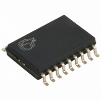
CY7C63723-SC Cypress Semiconductor Corp, CY7C63723-SC Datasheet - Page 19

CY7C63723-SC
Manufacturer Part Number
CY7C63723-SC
Description
IC MCU 8K LS USB/PS-2 18-SOIC
Manufacturer
Cypress Semiconductor Corp
Series
enCoRe™r
Specifications of CY7C63723-SC
Applications
USB Microcontroller
Core Processor
M8B
Program Memory Type
OTP (8 kB)
Controller Series
CY7C637xx
Ram Size
256 x 8
Interface
PS2, USB
Number Of I /o
10
Voltage - Supply
4 V ~ 5.5 V
Operating Temperature
0°C ~ 70°C
Mounting Type
Surface Mount
Package / Case
18-SOIC (7.5mm Width)
Lead Free Status / RoHS Status
Contains lead / RoHS non-compliant
Other names
428-1323
Available stocks
Company
Part Number
Manufacturer
Quantity
Price
Company:
Part Number:
CY7C63723-SC
Manufacturer:
CYPRESS
Quantity:
3 100
Company:
Part Number:
CY7C63723-SC
Manufacturer:
FUJI
Quantity:
154
Part Number:
CY7C63723-SC
Manufacturer:
CYPRESS/赛普拉斯
Quantity:
20 000
14.3
The CY7C637xx feature two non-control endpoints, endpoint
1 (EP1) and endpoint 2 (EP2). The EP1 and EP2 Mode
Registers do not have the locking mechanism of the EP0
Mode Register. The EP1 and EP2 Mode Registers use the
format shown in Figure 14-3. EP1 uses an 8-byte FIFO at
SRAM locations 0xF0–0xF7, EP2 uses an 8-byte FIFO at
SRAM locations 0xE8–0xEF as shown in Section 8.2.
Figure 14-3. USB Endpoint EP1, EP2 Mode Registers (Ad-
Bit 7: STALL
Bit [6:5]: Reserved. Must be written to zero during register
writes.
Bit 4: ACKed Transaction
Bit [3:0]: Mode Bit [3:0]
Document #: 38-08022 Rev. *B
Name
Read/
Reset
Write
Bit #
Bit
In addition, the Mode Bits are automatically changed by the
SIE in response to many USB transactions. For example, if
the Mode Bit [3:0] are set to 1011 which is ACK OUT-NAK
IN mode as shown in Table 22-1, the SIE will change the
endpoint Mode Bit [3:0] to NAK IN/OUT (0001) mode after
issuing an ACK handshake in response to an OUT token.
Firmware needs to update the mode for the SIE to respond
appropriately.
1 = The SIE will stall an OUT packet if the Mode Bits are set
to ACK-OUT, and the SIE will stall an IN packet if the mode
bits are set to ACK-IN. See Section 22.0 for the available
modes.
0 = This bit must be set to LOW for all other modes.
The ACKed transaction bit is set whenever the SIE engag-
es in a transaction to the register's endpoint that completes
with an ACK packet.
1 = The transaction completes with an ACK.
0 = The transaction does not complete with an ACK.
The EP1 and EP2 Mode Bits operate in the same manner
as the EP0 Mode Bits (see Section 14.2).
STALL Reserved
USB Non-control Endpoints
R/W
7
0
6
0
-
dresses 0x14 and 0x16)
5
0
-
Transaction
ACKed
R/C
4
0
FOR
FOR
R/W R/W R/W R/W
3
0
Mode Bit
2
0
1
0
0
0
14.4
There are three Endpoint Counter registers, with identical
formats for both control and non-control endpoints. These
registers contain byte count information for USB transactions,
as well as bits for data packet status. The format of these
registers is shown in Figure 14-4.
Bit 7: Data Toggle
Bit 6: Data Valid
Bit [5:4]: Reserved
Bit [3:0]: Byte Count Bit [3:0]
Read/Writ
Bit Name
This bit selects the DATA packet's toggle state. For IN
transactions, firmware must set this bit to the select the
transmitted Data Toggle. For OUT or SETUP transactions,
the hardware sets this bit to the state of the received Data
Toggle bit.
1 = DATA1
0 = DATA0
This bit is used for OUT and SETUP tokens only. This bit is
cleared to ‘0’ if CRC, bitstuff, or PID errors have occurred.
This bit does not update for some endpoint mode settings.
Refer to Table 22-3 for more details.
1 = Data is valid.
0 = Data is invalid. If enabled, the endpoint interrupt will
occur even if invalid data is received.
Byte Count Bits indicate the number of data bytes in a
transaction: For IN transactions, firmware loads the count
with the number of bytes to be transmitted to the host from
the endpoint FIFO. Valid values are 0 to 8 inclusive. For
OUT or SETUP transactions, the count is updated by hard-
ware to the number of data bytes received, plus 2 for the
CRC bytes. Valid values are 2 to 10 inclusive.
For Endpoint 0 Count Register, whenever the count up-
dates from a SETUP or OUT transaction, the count register
locks and cannot be written by the CPU. Reading the reg-
ister unlocks it. This prevents firmware from overwriting a
status update on incoming SETUP or OUT transactions be-
fore firmware has a chance to read the data.
Reset
Bit #
e
Figure 14-4. Endpoint 0,1,2 Counter Registers
USB Endpoint Counter Registers
(Addresses 0x11, 0x13 and 0x15)
Toggle
Data
R/W
7
0
Data
Valid
R/W
6
0
Reserved
5
0
-
4
0
-
CY7C63722
CY7C63723
CY7C63743
R/
W
3
0
Byte Count
Page 19 of 49
R/
W
2
0
R/
W
1
0
R/
W
0
0


