CY7C63723-SC Cypress Semiconductor Corp, CY7C63723-SC Datasheet - Page 26
CY7C63723-SC
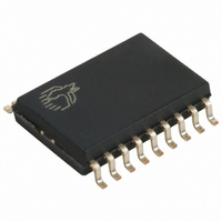
Manufacturer Part Number
CY7C63723-SC
Description
IC MCU 8K LS USB/PS-2 18-SOIC
Manufacturer
Cypress Semiconductor Corp
Series
enCoRe™r
Specifications of CY7C63723-SC
Applications
USB Microcontroller
Core Processor
M8B
Program Memory Type
OTP (8 kB)
Controller Series
CY7C637xx
Ram Size
256 x 8
Interface
PS2, USB
Number Of I /o
10
Voltage - Supply
4 V ~ 5.5 V
Operating Temperature
0°C ~ 70°C
Mounting Type
Surface Mount
Package / Case
18-SOIC (7.5mm Width)
Lead Free Status / RoHS Status
Contains lead / RoHS non-compliant
Other names
428-1323
Available stocks
Company
Part Number
Manufacturer
Quantity
Price
Company:

Part Number:
CY7C63723-SC
Manufacturer:
CYPRESS
Quantity:
3 100
Company:
Part Number:
CY7C63723-SC
Manufacturer:
FUJI
Quantity:
154
Part Number:
CY7C63723-SC
Manufacturer:
CYPRESS/赛普拉斯
Quantity:
20 000


Figure 19-6. Capture Timer Status Register (Address 0x45)
Bit [7:4]: Reserved.
Bit [3:0]: Capture A/B, Falling/Rising Event
Document #: 38-08022 Rev. *B
Name
Read/
Reset 0
Read/Write
Read/Write
Read/Write
Write
Bit #
Bit Name
Bit Name
Bit Name
Bit
These bits record the occurrence of any rising or falling
edges on the capture GPIO pins. Bits in this register are
cleared by reading the corresponding data register.
1 = A rising or falling event that matches the pin’s rising/fall-
ing condition has occurred.
0 = No event that matches the pin’s rising or falling edge
condition.
Because both Capture A events (rising and falling) share
an interrupt, user’s firmware needs to check the status of
both Capture A Falling and Rising Event bits to determine
what caused the interrupt. This is also true for Capture B
events.
Figure 19-5. Capture Timer B-Falling, Data Register
Figure 19-3. Capture Timer A-Falling, Data Register
Figure 19-4. Capture Timer B-Rising, Data Register
Reset
Reset
Reset
Bit #
Bit #
Bit #
7
-
Reserved
6
0
-
R
R
R
7
0
7
0
7
0
5
0
-
4
0
-
R
R
R
6
0
6
0
6
0
(Address 0x41)
(Address 0x43)
(Address 0x42)
Capture
Falling
Event
Capture A Falling Data
Capture B Falling Data
Capture B Rising Data
B
R
R
R
3
0
R
5
0
5
0
5
0
R
R
Capture
R
4
0
4
0
4
0
Rising
Event
B
R
2
0
FOR
FOR
R
R
R
3
0
3
0
3
0
Capture
Falling
Event
R
R
R
2
0
2
0
2
0
A
R
1
0
R
R
R
1
0
1
0
1
0
Capture
Rising
Event
R
A
0
0
R
R
0
0
R
0
0
0
0
Bit 7: First Edge Hold
Bit [6:4]: Prescale Bit [2:0]
Bit [3:0]: Capture A/B, Rising/Falling Interrupt Enable
Table 19-1. Capture Timer Prescalar Settings (Step size
and range for F
Name
Read/
Reset
Prescale
Write
Bit #
Bit
1 = The time of the first occurrence of an edge is held in the
Capture Timer Data Register until the data is read. Subse-
quent edges are ignored until the Capture Timer Data Reg-
ister is read.
0 = The time of the most recent edge is held in the Capture
Timer Data Register. That is, if multiple edges have oc-
curred before reading the capture timer, the time for the last
one will be read (default state).
The First Edge Hold function applies globally to all four cap-
ture timers.
Three prescaler bits allow the capture timer clock rate to be
selected among 5 choices, as shown in Table 19-1 below.
Each of the four Capture Timer registers can be individually
enabled to provide interrupts.
Both Capture A events share a common interrupt request,
as do the two Capture B events. In addition to the event
enables, the main Capture Interrupt Enables bit in the Glo-
bal Interrupt Enable register (Section 21.0) must be set to
activate a capture interrupt.
1 = Enable interrupt
0 = Disable interrupt
000
001
010
100
011
2:0
Figure 19-7. Capture Timer Configuration Register
Edge
Hold
First
R/W R/W R/W R/W
7
0
Bits 7:0 of free-running timer
Bits 8:1 of free-running timer
Bits 9:2 of free-running timer
Bits 10:3 of free-running timer
Bits 11:4 of free-running timer
Prescale Bit
6
0
CLK
Captured Bits
[2:0]
5
0
= 6 MHz)
(Address 0x44)
4
0
Capture
Enable
Falling
R/W
Int
B
3
0
Capture
Enable
Rising
R/W
Int
B
2
0
CY7C63722
CY7C63723
CY7C63743
16 µs 4.096 ms
Step
LSB
Size
1 µs
2 µs
4 µs
8 µs
Capture
Enable
Falling
Page 26 of 49
R/W
Int
A
1
0
1.024 ms
2.048 ms
Range
256 µs
512 µs
Capture
Enable
Rising
R/W
Int
0
A
0
Related parts for CY7C63723-SC
Image
Part Number
Description
Manufacturer
Datasheet
Request
R

Part Number:
Description:
Manufacturer:
Cypress Semiconductor Corp
Datasheet:
Part Number:
Description:
Manufacturer:
Cypress Semiconductor Corp
Datasheet:
Part Number:
Description:
Manufacturer:
Cypress Semiconductor Corp
Datasheet:
Part Number:
Description:
Manufacturer:
Cypress Semiconductor Corp
Datasheet:
Part Number:
Description:
Manufacturer:
Cypress Semiconductor Corp
Datasheet: