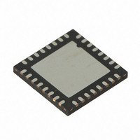
CY8CTMG201-32LQXI Cypress Semiconductor Corp, CY8CTMG201-32LQXI Datasheet - Page 226

CY8CTMG201-32LQXI
Manufacturer Part Number
CY8CTMG201-32LQXI
Description
IC MCU 16K FLASH PSOC 32UQFN
Manufacturer
Cypress Semiconductor Corp
Series
TrueTouch™r
Datasheet
1.CY8CTST200-16LGXI.pdf
(308 pages)
Specifications of CY8CTMG201-32LQXI
Applications
Touchscreen Controller
Core Processor
M8C
Program Memory Type
FLASH (16 kB)
Controller Series
CY8CT
Ram Size
2K x 8
Interface
I²C, SPI, UART/USART, USB
Number Of I /o
28
Voltage - Supply
1.8 V
Operating Temperature
-40°C ~ 85°C
Mounting Type
Surface Mount
Package / Case
32-UQFN Exposed Pad, 32-HUQFN, 32-SQFN
Processor Series
CY8CTxx2xx
Core
M8C
For Use With
770-1000 - ISP 4PORT FOR CYPRESS PSOC MCU
Lead Free Status / RoHS Status
Lead free / RoHS Compliant
Other names
428-2971
- Current page: 226 of 308
- Download datasheet (3Mb)
I2C_XCFG
21.3.38 I2C_XCFG
This register configures enhanced features. The Enable bit (bit 0) of the
the I2C enhanced features to work.
In the table above, note that reserved bits are grayed table cells and are not described in the bit description section below.
Always write reserved bits with a value of ‘0’. For additional information, refer to the
I2C Slave chapter .
Bit
3
1
0
226
Individual Register Names and Addresses:
I2C_XCFG: 0,C8h
Access : POR
Bit Name
0,C8h
Buffer Mode
No BC Int
HW Addr En
Name
I
2
C Extended Configuration Register
7
6
Description
In compatibility mode, every received or transmitted byte generates a Byte Complete Interrupt. This is
also true in buffered mode regardless of whether the bus is stalled or not.
Note When this bit is set to a ‘1’, A BC interrupt is not enabled for any data byte that is automatically
ACK’ed (i.e., does not require the bus to stall). A BC interrupt is always generated upon any stall so
the CPU takes the appropriate action. When the bit is set, it is possible to implement packet transfers
without CPU intervention by enabling an interrupt upon the Stop detect.
This bit determines the operation mode of the enhanced buffer module. The following table describes
the available modes.
When this bit is set to a ‘1’, hardware address compare is enabled. When enabled, bit 3 in the
I2C_SCR register is not set. Upon a compare, the address is automatically ACK’ed, and upon a mis-
match, the address is automatically NACK’ed and the hardware reverts to an idle state waiting for the
next Start detection. You must configure the compare address in the I2C_ADDR register. When this
bit is a ‘0’, bit 3 of the I2C_SCR register is set and the bus stalls, and the received address is avail-
able in the I2C_DR register to enable the CPU to do a firmware address compare. The functionality of
this bit is independent of the data buffering mode.
0
1
Buffer
Mode
PSoC CY8CTMG20x and CY8CTST200 TRM, Document No. 001-53603 Rev. *C
Compatible
EZI2C
Name
5
There is no buffering in the default compatibility
mode. The I2C bus is stalled upon every received
or transmitted byte, including address bytes. The
CPU is required to process the interrupt and write or
read the data and status as required to continue the
operation.
The I2C slave appears as a 32-byte RAM interface
to an external master. A specific protocol must be
followed, in which the master controls the RAM
pointer for both read and write operations. The I2C
bus is never stalled. Receive ACKs are automati-
cally generated. The CPU is responsible for putting
valid data into the RAM for external reads, and for
reading received data.
4
Description
No BC Int
RW : 0
I2C_CFG
3
(0,D6h) register should be set to 1'b1 for
Register Definitions on page 122
2
0,C8h
Buffer Mode
RW : 0
1
HW Addr En
RW : 0
0
in the
[+] Feedback
Related parts for CY8CTMG201-32LQXI
Image
Part Number
Description
Manufacturer
Datasheet
Request
R
Part Number:
Description:
IC MCU 16K FLASH PSOC 48-QFN
Manufacturer:
Cypress Semiconductor Corp
Datasheet:
Part Number:
Description:
IC MCU 16K FLASH PSOC 32UQFN
Manufacturer:
Cypress Semiconductor Corp
Part Number:
Description:
IC MCU 16K FLASH PSOC 48-QFN
Manufacturer:
Cypress Semiconductor Corp
Part Number:
Description:
Manufacturer:
Cypress Semiconductor Corp
Datasheet:
Part Number:
Description:
Manufacturer:
Cypress Semiconductor Corp
Datasheet:
Part Number:
Description:
Manufacturer:
Cypress Semiconductor Corp
Datasheet:
Part Number:
Description:
Manufacturer:
Cypress Semiconductor Corp
Datasheet:


