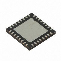
CY8CTMG201-32LQXI Cypress Semiconductor Corp, CY8CTMG201-32LQXI Datasheet - Page 78

CY8CTMG201-32LQXI
Manufacturer Part Number
CY8CTMG201-32LQXI
Description
IC MCU 16K FLASH PSOC 32UQFN
Manufacturer
Cypress Semiconductor Corp
Series
TrueTouch™r
Datasheet
1.CY8CTST200-16LGXI.pdf
(308 pages)
Specifications of CY8CTMG201-32LQXI
Applications
Touchscreen Controller
Core Processor
M8C
Program Memory Type
FLASH (16 kB)
Controller Series
CY8CT
Ram Size
2K x 8
Interface
I²C, SPI, UART/USART, USB
Number Of I /o
28
Voltage - Supply
1.8 V
Operating Temperature
-40°C ~ 85°C
Mounting Type
Surface Mount
Package / Case
32-UQFN Exposed Pad, 32-HUQFN, 32-SQFN
Processor Series
CY8CTxx2xx
Core
M8C
For Use With
770-1000 - ISP 4PORT FOR CYPRESS PSOC MCU
Lead Free Status / RoHS Status
Lead free / RoHS Compliant
Other names
428-2971
- Current page: 78 of 308
- Download datasheet (3Mb)
10.3.3
The Sleep Configuration Register (SLP_CFG2) holds the
configuration for I2C sleep, deep sleep, and buzz.
Bits 3 and 2: ALT_Buzz[1:0]. These bits control additional
selections for POR/LVD buzz rates. These are lower rates
than the compatibility mode to provide for lower average
power.
‘00’ - Compatibility mode, buzz rate determined by PSSDC
bits.
‘01’ - Duty cycle is 1/32768.
‘10’ - Duty cycle is 1/8192.
‘11’ - Reserved.
Bit 1: I2C_ON. This bit enables the standby regulator in
sleep at a level sufficient to supply the I2C circuitry. It is
independent of the LSO_OFF bit.
10.3.4
The Sleep Configuration Register (SLP_CFG3) holds the
configuration of the wakeup sequence taps.
It is strongly recommended to not alter this register set-
ting.
Bit 6: DBL_TAPS. When this bit is set, all the tap values
(T0, T1, and T2) are doubled for the wakeup sequence.
Bits 5 and 4: T2TAP[1:0]. These bits control the duration
of the T2-T4 sequence (see
selecting a tap from the WakeupTimer. Note The T2 delay is
only valid for the wakeup sequence. It is not used for the
buzz sequence.
‘00’ - 1 µs
‘01’ - 2 µs
‘10’ - 5 µs
‘11’ - 10 µs
10.3.5
■
■
■
■
Sleep and Watchdog
78
1,ECh
1,EDh
Address
Address
INT_MSK0 Register on page
OSC_CR0 Register on page
ILO_TR Register on page
CPU_SCR0 Register on page
SLP_CFG2
SLP_CFG3
SLP_CFG2 Register
SLP_CFG3 Register
Related Registers
Name
Name
Bit 7
Bit 7
68.
Figure 10-2 on page
113.
51.
138.
DBL_TAPS
Bit 6
Bit 6
PSoC CY8CTMG20x and CY8CTST200 TRM, Document No. 001-53603 Rev. *C
Bit 5
Bit 5
T2TAP [1:0]
75) by
Bit 4
Bit 4
Bit 0: LSO_OFF: This bit disables the LSO oscillator when
in sleep state. By default, the LSO oscillator runs in sleep.
When this bit is ‘0’, the standby regulator is active at a power
level to supply the LSO and Sleep timer circuitry and the
LSO is enabled. When this bit is ‘1’, the LSO is disabled in
sleep, which in turn, disables the Sleep Timer, Watchdog
Timer, and POR/LVD buzzing activity in sleep. If I2C_ON is
not enabled and this bit is set, the device is in the lowest
power deep sleep mode. Only a GPIO interrupt awakens the
device from deep sleep mode.
For additional information, refer to the
on page
Bits 3 and 2: T1TAP[1:0]. These bits control the duration of
the T1-T2 sequence (see
ing a tap from the Wakeup Timer.
‘00’ - 3 µs
01’ - 4 µs
‘10’ - 5 µs
‘11’ - 10 µs
Bits 1 and 0: T0TAP[1:0]. These bits control the duration
of the T0-T1 sequence (see
selecting a tap from the Wakeup Timer.
‘00’ - 10 µs
‘01’ - 14 µs
‘10’ - 20 µs
‘11’ - 30 µs
For additional information, refer to the
on page
■
CPU_SCR1 Register on page
Bit 3
Bit 3
ALT_Buzz [1:0]
284.
285.
T1TAP [1:0]
Bit 2
Bit 2
Figure 10-2 on page
I2C_ON
Bit 1
Bit 1
Figure 10-2 on page
T0TAP [1:0]
137.
LSO_OFF
SLP_CFG2 register
SLP_CFG3 register
Bit 0
Bit 0
75) by select-
RW : 0x7F
Access
RW : 00
Access
75) by
[+] Feedback
Related parts for CY8CTMG201-32LQXI
Image
Part Number
Description
Manufacturer
Datasheet
Request
R
Part Number:
Description:
IC MCU 16K FLASH PSOC 48-QFN
Manufacturer:
Cypress Semiconductor Corp
Datasheet:
Part Number:
Description:
IC MCU 16K FLASH PSOC 32UQFN
Manufacturer:
Cypress Semiconductor Corp
Part Number:
Description:
IC MCU 16K FLASH PSOC 48-QFN
Manufacturer:
Cypress Semiconductor Corp
Part Number:
Description:
Manufacturer:
Cypress Semiconductor Corp
Datasheet:
Part Number:
Description:
Manufacturer:
Cypress Semiconductor Corp
Datasheet:
Part Number:
Description:
Manufacturer:
Cypress Semiconductor Corp
Datasheet:
Part Number:
Description:
Manufacturer:
Cypress Semiconductor Corp
Datasheet:


