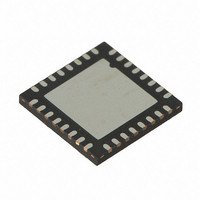
CY8CTMG201-32LQXI Cypress Semiconductor Corp, CY8CTMG201-32LQXI Datasheet - Page 42

CY8CTMG201-32LQXI
Manufacturer Part Number
CY8CTMG201-32LQXI
Description
IC MCU 16K FLASH PSOC 32UQFN
Manufacturer
Cypress Semiconductor Corp
Series
TrueTouch™r
Datasheet
1.CY8CTST200-16LGXI.pdf
(308 pages)
Specifications of CY8CTMG201-32LQXI
Applications
Touchscreen Controller
Core Processor
M8C
Program Memory Type
FLASH (16 kB)
Controller Series
CY8CT
Ram Size
2K x 8
Interface
I²C, SPI, UART/USART, USB
Number Of I /o
28
Voltage - Supply
1.8 V
Operating Temperature
-40°C ~ 85°C
Mounting Type
Surface Mount
Package / Case
32-UQFN Exposed Pad, 32-HUQFN, 32-SQFN
Processor Series
CY8CTxx2xx
Core
M8C
For Use With
770-1000 - ISP 4PORT FOR CYPRESS PSOC MCU
Lead Free Status / RoHS Status
Lead free / RoHS Compliant
Other names
428-2971
- Current page: 42 of 308
- Download datasheet (3Mb)
4.2
The following registers are associated with RAM Paging and are listed in address order. The register descriptions have an
associated register table showing the bit structure for that register. The bits in the tables that are grayed out are reserved bits
and are not detailed in the register descriptions that follow. Always write reserved bits with a value of ‘0‘. For a complete table
of RAM Paging registers, refer to the
4.2.1
The Temporary Data Registers (TMP_DR0, TMP_DR1,
TMP_DR2, and TMP_DR3) enhance the performance in
multiple SRAM page PSoC devices.
These registers have no predefined function (for example,
the compiler and hardware do not use these registers) and
exist for the user to define.
Bits 7 to 0: Data[7:0]. Due to the paged SRAM architec-
ture of PSoC devices with more than 256 bytes of SRAM, a
4.2.2
The Current Page Pointer Register (CUR_PP) sets the
effective SRAM page for normal memory accesses in a
multi-SRAM page PSoC device.
Bits 2 to 0: Page Bits[2:0]. These bits affect the SRAM
page that is accessed by an instruction when the
CPU_F[7:6] bits have a value of either 10b or 11b. Source
Indexed, Destination Indexed addressing modes, and stack
instructions, are never affected by the value of the CUR_PP
register. (See the STK_PP and IDX_PP registers for more
information.)
RAM Paging
42
x,6xh
LEGEND
x An ‘x’ before the comma in the address field indicates that this register can be read or written to no matter what bank is used. An “x” after the comma in the
0,D0h
Address
Address
address field indicates that there are multiple instances of the register.
Register Definitions
TMP_DRx
CUR_PP
TMP_DRx Registers
CUR_PP Register
Name
Name
Bit 7
Bit 7
Summary Table of the Core Registers on page
Bit 6
Bit 6
PSoC CY8CTMG20x and CY8CTST200 TRM, Document No. 001-53603 Rev. *C
Bit 5
Bit 5
Bit 4
Bit 4
Data[7:0]
value in SRAM is not always accessible without first chang-
ing the current page. The TMP_DRx registers are readable
and writable registers that are provided to improve the per-
formance of multiple SRAM page PSoC devices, by supply-
ing some register space for data that is always accessible.
For an expanded listing of the TMP_DRx registers, refer to
the
additional information, refer to the
page
The Source Indirect Post Increment and Destination Indirect
Post Increment addressing modes, better know as MVI, are
only partially affected by the value of the CUR_PP register.
For MVI instructions, the pointer address is in the SRAM
page indicated by CUR_PP, but the address pointed to may
be in another SRAM page.
See the MVR_PP and MVW_PP register descriptions for
more information.
For additional information, refer to the
page
Summary Table of the Core Registers on page
266.
234.
Bit 3
Bit 3
Bit 2
Bit 2
24.
Page Bits[2:0]
Bit 1
Bit 1
TMP_DRx register on
CUR_PP register on
Bit 0
Bit 0
Access
RW : 00
Access
RW : 00
24. For
[+] Feedback
Related parts for CY8CTMG201-32LQXI
Image
Part Number
Description
Manufacturer
Datasheet
Request
R
Part Number:
Description:
IC MCU 16K FLASH PSOC 48-QFN
Manufacturer:
Cypress Semiconductor Corp
Datasheet:
Part Number:
Description:
IC MCU 16K FLASH PSOC 32UQFN
Manufacturer:
Cypress Semiconductor Corp
Part Number:
Description:
IC MCU 16K FLASH PSOC 48-QFN
Manufacturer:
Cypress Semiconductor Corp
Part Number:
Description:
Manufacturer:
Cypress Semiconductor Corp
Datasheet:
Part Number:
Description:
Manufacturer:
Cypress Semiconductor Corp
Datasheet:
Part Number:
Description:
Manufacturer:
Cypress Semiconductor Corp
Datasheet:
Part Number:
Description:
Manufacturer:
Cypress Semiconductor Corp
Datasheet:


