MPC755CRX400LE Freescale Semiconductor, MPC755CRX400LE Datasheet - Page 12
MPC755CRX400LE
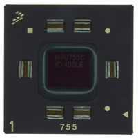
Manufacturer Part Number
MPC755CRX400LE
Description
IC MPU 32BIT 400MHZ PPC 360-CBGA
Manufacturer
Freescale Semiconductor
Datasheet
1.MPC755BPX300LE.pdf
(56 pages)
Specifications of MPC755CRX400LE
Processor Type
MPC7xx PowerPC 32-Bit
Speed
400MHz
Voltage
2V
Mounting Type
Surface Mount
Package / Case
360-FCCBGA
Family Name
MPC7xx
Device Core
PowerPC
Device Core Size
64b
Frequency (max)
400MHz
Instruction Set Architecture
RISC
Supply Voltage 1 (typ)
2V
Operating Supply Voltage (max)
2.1V
Operating Supply Voltage (min)
1.9V
Operating Temp Range
0C to 105C
Operating Temperature Classification
Commercial
Mounting
Surface Mount
Pin Count
360
Package Type
FCCBGA
Lead Free Status / RoHS Status
Contains lead / RoHS non-compliant
Features
-
Lead Free Status / Rohs Status
Not Compliant
Available stocks
Company
Part Number
Manufacturer
Quantity
Price
Company:

Part Number:
MPC755CRX400LE
Manufacturer:
MOT
Quantity:
12 388
Company:
Part Number:
MPC755CRX400LE
Manufacturer:
Freescale Semiconductor
Quantity:
10 000


Electrical and Thermal Characteristics
4.2
This section provides the AC electrical characteristics for the MPC755. After fabrication, functional parts
are sorted by maximum processor core frequency as shown in
and tested for conformance to the AC specifications for that frequency. The processor core frequency is
determined by the bus (SYSCLK) frequency and the settings of the PLL_CFG[0:3] signals. Parts are sold
by maximum processor core frequency; see
4.2.1
Table 8
12
At recommended operating conditions (see
Processor frequency
VCO frequency
SYSCLK frequency
SYSCLK cycle time
SYSCLK rise and fall time
SYSCLK duty cycle measured at
OV
SYSCLK jitter
Internal PLL relock time
Notes:
1. Caution: The SYSCLK frequency and PLL_CFG[0:3] settings must be chosen such that the resulting SYSCLK (bus)
2. Rise and fall times measurements are now specified in terms of slew rates, rather than time to account for selectable I/O bus
3. Timing is guaranteed by design and characterization.
4. This represents total input jitter—short term and long term combined—and is guaranteed by design.
5. Relock timing is guaranteed by design and characterization. PLL-relock time is the maximum amount of time required for PLL
frequency, CPU (core) frequency, and PLL (VCO) frequency do not exceed their respective maximum or minimum operating
frequencies. Refer to the PLL_CFG[0:3] signal description in
settings.
interface levels. The minimum slew rate of 1 V/ns is equivalent to a 2 ns maximum rise/fall time measured at 0.4 and 2.4 V
(OV
lock after a stable V
the PLL has been disabled and subsequently re-enabled during sleep mode. Also note that HRESET must be held asserted
for a minimum of 255 bus clocks after the PLL-relock time during the power-on reset sequence.
DD
/2
DD
provides the clock AC timing specifications as defined in
Characteristic
= 3.3 V) or a rise/fall time of 1 ns measured at 0.4 and 1.8 V (OV
AC Electrical Characteristics
Clock AC Specifications
DD
and SYSCLK are reached during the power-on reset sequence. This specification also applies when
MPC755 RISC Microprocessor Hardware Specifications, Rev. 8
Symbol
f
t
t
t
t
SYSCLK
SYSCLK
SYSCLK
KR
KR
t
Table
KHKL
Table 8. Clock AC Timing Specifications
f
f
VCO
core
, t
, t
KF
KF
/
3)
Min
200
400
25
10
—
—
40
—
—
Section 10, “Ordering Information.”
300 MHz
Maximum Processor Core Frequency
±150
Max
300
600
100
100
2.0
1.4
40
60
Section 8.1, “PLL Configuration
Min
200
400
25
10
40
—
—
—
—
350 MHz
DD
Section 4.2.1, “Clock AC Specifications,”
= 2.5 V).
Figure
±150
Max
350
700
100
100
2.0
1.4
40
60
3.
Min
200
400
25
10
40
—
—
—
—
400 MHz
,”
for valid PLL_CFG[0:3]
±150
Freescale Semiconductor
Max
400
800
100
100
2.0
1.4
40
60
MHz
MHz
MHz
Unit
ns
ns
ns
ps
μs
%
Notes
3, 4
3, 5
1
1
1
2
2
3
Related parts for MPC755CRX400LE
Image
Part Number
Description
Manufacturer
Datasheet
Request
R

Part Number:
Description:
Host Processor
Manufacturer:
Motorola Semiconductor Products
Datasheet:

Part Number:
Description:
Manufacturer:
Freescale Semiconductor, Inc
Datasheet:
Part Number:
Description:
Manufacturer:
Freescale Semiconductor, Inc
Datasheet:
Part Number:
Description:
Manufacturer:
Freescale Semiconductor, Inc
Datasheet:
Part Number:
Description:
Manufacturer:
Freescale Semiconductor, Inc
Datasheet:
Part Number:
Description:
Manufacturer:
Freescale Semiconductor, Inc
Datasheet:
Part Number:
Description:
Manufacturer:
Freescale Semiconductor, Inc
Datasheet:
Part Number:
Description:
Manufacturer:
Freescale Semiconductor, Inc
Datasheet:
Part Number:
Description:
Manufacturer:
Freescale Semiconductor, Inc
Datasheet:
Part Number:
Description:
Manufacturer:
Freescale Semiconductor, Inc
Datasheet:
Part Number:
Description:
Manufacturer:
Freescale Semiconductor, Inc
Datasheet:
Part Number:
Description:
Manufacturer:
Freescale Semiconductor, Inc
Datasheet:
Part Number:
Description:
Manufacturer:
Freescale Semiconductor, Inc
Datasheet:
Part Number:
Description:
Manufacturer:
Freescale Semiconductor, Inc
Datasheet:
Part Number:
Description:
Manufacturer:
Freescale Semiconductor, Inc
Datasheet: