MPC755CRX400LE Freescale Semiconductor, MPC755CRX400LE Datasheet - Page 4
MPC755CRX400LE
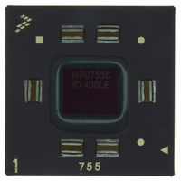
Manufacturer Part Number
MPC755CRX400LE
Description
IC MPU 32BIT 400MHZ PPC 360-CBGA
Manufacturer
Freescale Semiconductor
Datasheet
1.MPC755BPX300LE.pdf
(56 pages)
Specifications of MPC755CRX400LE
Processor Type
MPC7xx PowerPC 32-Bit
Speed
400MHz
Voltage
2V
Mounting Type
Surface Mount
Package / Case
360-FCCBGA
Family Name
MPC7xx
Device Core
PowerPC
Device Core Size
64b
Frequency (max)
400MHz
Instruction Set Architecture
RISC
Supply Voltage 1 (typ)
2V
Operating Supply Voltage (max)
2.1V
Operating Supply Voltage (min)
1.9V
Operating Temp Range
0C to 105C
Operating Temperature Classification
Commercial
Mounting
Surface Mount
Pin Count
360
Package Type
FCCBGA
Lead Free Status / RoHS Status
Contains lead / RoHS non-compliant
Features
-
Lead Free Status / Rohs Status
Not Compliant
Available stocks
Company
Part Number
Manufacturer
Quantity
Price
Company:

Part Number:
MPC755CRX400LE
Manufacturer:
MOT
Quantity:
12 388
Company:
Part Number:
MPC755CRX400LE
Manufacturer:
Freescale Semiconductor
Quantity:
10 000


Features
4
•
•
•
•
— Three-cycle latency, one-cycle throughput, double-precision add
— Four-cycle latency, two-cycle throughput, double-precision multiply-add
System unit
— Executes CR logical instructions and miscellaneous system instructions
— Special register transfer instructions
Load/store unit
— One-cycle load or store cache access (byte, half-word, word, double word)
— Effective address generation
— Hits under misses (one outstanding miss)
— Single-cycle unaligned access within double-word boundary
— Alignment, zero padding, sign extend for integer register file
— Floating-point internal format conversion (alignment, normalization)
— Sequencing for load/store multiples and string operations
— Store gathering
— Cache and TLB instructions
— Big- and little-endian byte addressing supported
Level 1 cache structure
— 32K, 32-byte line, eight-way set-associative instruction cache (iL1)
— 32K, 32-byte line, eight-way set-associative data cache (dL1)
— Cache locking for both instruction and data caches, selectable by group of ways
— Single-cycle cache access
— Pseudo least-recently-used (PLRU) replacement
— Copy-back or write-through data cache (on a page per page basis)
— MEI data cache coherency maintained in hardware
— Nonblocking instruction and data cache (one outstanding miss under hits)
— No snooping of instruction cache
Level 2 (L2) cache interface (not implemented on MPC745)
— Internal L2 cache controller and tags; external data SRAMs
— 256K, 512K, and 1 Mbyte two-way set-associative L2 cache support
— Copy-back or write-through data cache (on a page basis, or for all L2)
— Instruction-only mode and data-only mode
— 64-byte (256K/512K) or 128-byte (1M) sectored line size
— Supports flow through (register-buffer) synchronous BurstRAMs, pipelined (register-register)
— L2 configurable to cache, private memory, or split cache/private memory
— Core-to-L2 frequency divisors of ÷1, ÷1.5, ÷2, ÷2.5, and ÷3 supported
— 64-bit data bus
synchronous BurstRAMs (3-1-1-1 or strobeless 4-1-1-1) and pipelined (register-register) late
write synchronous BurstRAMs
MPC755 RISC Microprocessor Hardware Specifications, Rev. 8
Freescale Semiconductor
Related parts for MPC755CRX400LE
Image
Part Number
Description
Manufacturer
Datasheet
Request
R

Part Number:
Description:
Host Processor
Manufacturer:
Motorola Semiconductor Products
Datasheet:

Part Number:
Description:
Manufacturer:
Freescale Semiconductor, Inc
Datasheet:
Part Number:
Description:
Manufacturer:
Freescale Semiconductor, Inc
Datasheet:
Part Number:
Description:
Manufacturer:
Freescale Semiconductor, Inc
Datasheet:
Part Number:
Description:
Manufacturer:
Freescale Semiconductor, Inc
Datasheet:
Part Number:
Description:
Manufacturer:
Freescale Semiconductor, Inc
Datasheet:
Part Number:
Description:
Manufacturer:
Freescale Semiconductor, Inc
Datasheet:
Part Number:
Description:
Manufacturer:
Freescale Semiconductor, Inc
Datasheet:
Part Number:
Description:
Manufacturer:
Freescale Semiconductor, Inc
Datasheet:
Part Number:
Description:
Manufacturer:
Freescale Semiconductor, Inc
Datasheet:
Part Number:
Description:
Manufacturer:
Freescale Semiconductor, Inc
Datasheet:
Part Number:
Description:
Manufacturer:
Freescale Semiconductor, Inc
Datasheet:
Part Number:
Description:
Manufacturer:
Freescale Semiconductor, Inc
Datasheet:
Part Number:
Description:
Manufacturer:
Freescale Semiconductor, Inc
Datasheet:
Part Number:
Description:
Manufacturer:
Freescale Semiconductor, Inc
Datasheet: