A80386DX16 Intel, A80386DX16 Datasheet - Page 28
A80386DX16
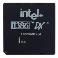
Manufacturer Part Number
A80386DX16
Description
IC MPU 32-BIT 5V 16MHZ 132-PGA
Manufacturer
Intel
Datasheet
1.A80386DX16.pdf
(139 pages)
Specifications of A80386DX16
Processor Type
386DX
Features
32-bit
Speed
16MHz
Voltage
5V
Mounting Type
Surface Mount
Package / Case
132-PGA
Family Name
Intel386 DX
Device Core Size
32b
Frequency (max)
16MHz
Supply Voltage 1 (typ)
5V
Operating Supply Voltage (max)
5.25V
Operating Supply Voltage (min)
4.75V
Operating Temp Range
0C to 85C
Operating Temperature Classification
Commercial
Mounting
Through Hole
Pin Count
132
Package Type
PGA
Lead Free Status / RoHS Status
Contains lead / RoHS non-compliant
Other names
807050
Available stocks
Company
Part Number
Manufacturer
Quantity
Price


Intel386
2 11 TESTABILITY
2 11 1 Self-Test
The Intel386 DX has the capability to perform a self-
test The self-test checks the function of all of the
Control ROM and most of the non-random logic of
the part Approximately one-half of the Intel386 DX
can be tested during self-test
Self-Test is initiated on the Intel386 DX when the
RESET pin transitions from HIGH to LOW and the
BUSY
clocks or approximately 26 milliseconds with a
20 MHz Intel386 DX At the completion of self-test
the processor performs reset and begins normal op-
eration The part has successfully passed self-test if
the contents of the EAX register are zero (0) If the
results of EAX are not zero then the self-test has
detected a flaw in the part
2 11 2 TLB Testing
The Intel386 DX provides a mechanism for testing
the Translation Lookaside Buffer (TLB) if desired
This particular mechanism is unique to the Intel386
DX and may not be continued in the same way in
future processors When testing the TLB paging
must be turned off (PG
TLB testing hardware and avoid interference with
the test data being written to the TLB
There are two TLB testing operations 1) write en-
tries into the TLB and 2) perform TLB lookups Two
Test Registers shown in Figure 2-12 are provided
for the purpose of testing TR6 is the ‘‘test command
register’’ and TR7 is the ‘‘test data register’’ The
fields within these registers are defined below
C This is the command bit For a write into TR6 to
cause an immediate write into the TLB entry write a
0 to this bit For a write into TR6 to cause an immedi-
ate TLB lookup write a 1 to this bit
Linear Address This is the tag field of the TLB On
a TLB write a TLB entry is allocated to this linear
address and the rest of that TLB entry is set per the
value of TR7 and the value just written into TR6 On
a TLB lookup the TLB is interrogated per this value
and if one and only one TLB entry matches the rest
of the fields of TR6 and TR7 are set from the match-
ing TLB entry
Physical Address This is the data field of the TLB
On a write to the TLB the TLB entry allocated to the
linear address in TR6 is set to this value On a TLB
lookup the data field (physical address) from the
TLB is read out to here
28
pin is low The self-test takes about 2 19
TM
DX MICROPROCESSOR
e
0 in CR0) to enable the
PL On a TLB write PL
TR7 to select which of four associative blocks of the
TLB is to be written but PL
pointer in the paging unit to select which TLB block
is written On a TLB lookup the PL bit indicates
whether the lookup was a hit (PL gets set to 1) or a
miss (PL gets reset to 0)
V The valid bit for this TLB entry All valid bits can
also be cleared by writing to CR3
D D
U U
W W
For D U and W both the attribute and its comple-
ment are provided as tag bits to permit the option of
a ‘‘don’t care’’ on TLB lookups The meaning of
these pairs of bits is given in the following table
For writing a TLB entry
1 Write TR7 for the desired physical address PL
2 Write TR6 with the appropriate linear address
For looking up (reading) a TLB entry
1 Write TR6 with the appropriate linear address (be
2 Read TR7 and TR6 If the PL bit in TR7 indicates
2 12 DEBUGGING SUPPORT
The Intel386 DX provides several features which
simplify the debugging process The three catego-
ries of on-chip debugging aids are
1) the code execution breakpoint opcode (0CCH)
2) the single-step capability provided by the TF bit in
3) the code and data breakpoint capability provided
X X
0
0
1
1
and REP values
etc (be sure to write C
mand)
sure to write C
a hit then the other values reveal the TLB con-
tents If PL indicates a miss then the other values
in TR7 and TR6 are indeterminate
the flag register and
by the Debug Registers DR0-3 DR6 and DR7
0
1
0
1
The dirty bit for from the TLB entry
The user bit for from the TLB entry
The writable bit for from the TLB entry
Match if X
Match if X
Effect During
TLB Lookup
Match all
Miss All
e
1 for ‘‘lookup’’ command)
e
e
0
1
e
Bit X Becomes Undefined
Bit X Becomes Undefined
1 causes the REP field of
e
e
X after TLB Write
Bit X Becomes 0
Bit X Becomes 1
0 allows the internal
Value of Bit
0 for ‘‘write’’ com-
Related parts for A80386DX16
Image
Part Number
Description
Manufacturer
Datasheet
Request
R

Part Number:
Description:
Microprocessor: Intel Celeron M Processor 320 and Ultra Low Voltage Intel Celeron M Processor at 600MHz
Manufacturer:
Intel Corporation
Part Number:
Description:
Intel 82550 Fast Ethernet Multifunction PCI/CardBus Controller
Manufacturer:
Intel Corporation
Datasheet:
Part Number:
Description:
Intel StrataFlash memory 32 Mbit. Access speed 120 ns
Manufacturer:
Intel Corporation
Datasheet:
Part Number:
Description:
Intel StrataFlash memory 32 Mbit. Access speed 120 ns
Manufacturer:
Intel Corporation
Datasheet:
Part Number:
Description:
Intel StrataFlash memory 64 Mbit. Access speed 150 ns
Manufacturer:
Intel Corporation
Datasheet:
Part Number:
Description:
Intel StrataFlash memory 32 Mbit. Access speed 100 ns
Manufacturer:
Intel Corporation
Datasheet:
Part Number:
Description:
DA28F640J5A-1505 Volt Intel StrataFlash Memory
Manufacturer:
Intel Corporation
Datasheet:
Part Number:
Description:
5 Volt Intel StrataFlash?? Memory
Manufacturer:
Intel Corporation
Datasheet:
Part Number:
Description:
5 Volt Intel StrataFlash?? Memory
Manufacturer:
Intel Corporation
Part Number:
Description:
Intel 6300ESB I/O Controller Hub
Manufacturer:
Intel Corporation
Datasheet:
Part Number:
Description:
Intel 82801DB I/O Controller Hub (ICH4), Pb-Free SLI
Manufacturer:
Intel Corporation
Datasheet:
Part Number:
Description:
Intel 82801FB I/O Controller Hub (ICH6)
Manufacturer:
Intel Corporation
Datasheet:
Part Number:
Description:
Intel Strataflash Memory28F128J3 28F640J3 28F320J3
Manufacturer:
Intel Corporation
Datasheet:
Part Number:
Description:
Controllers, Intel 430TX PCIset: 82439TX System Controller (MTXC)
Manufacturer:
Intel Corporation