MPC8379EVRAJF Freescale Semiconductor, MPC8379EVRAJF Datasheet - Page 106
MPC8379EVRAJF
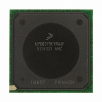
Manufacturer Part Number
MPC8379EVRAJF
Description
MPU PWRQUICC II 533MHZ 689TEPBGA
Manufacturer
Freescale Semiconductor
Series
PowerQUICC II PROr
Datasheets
1.MPC8377EVRAGD.pdf
(126 pages)
2.MPC8377EVRAGD.pdf
(2 pages)
3.MPC8379VRAGD.pdf
(116 pages)
Specifications of MPC8379EVRAJF
Processor Type
MPC83xx PowerQUICC II Pro 32-Bit
Speed
533MHz
Voltage
1V
Mounting Type
Surface Mount
Package / Case
689-TePBGA II
Maximum Clock Frequency
533 MHz
Operating Supply Voltage
1.8 V to 2.5 V
Maximum Operating Temperature
+ 105 C
Mounting Style
SMD/SMT
I/o Voltage
1.8 V, 2.5 V, 3.3 V
Minimum Operating Temperature
0 C
Core Size
32 Bit
Program Memory Size
64KB
Cpu Speed
533MHz
Embedded Interface Type
DUART, HSSI, I2C, IPIC, JTAG, SPI, USB
Digital Ic Case Style
BGA
No. Of Pins
689
Rohs Compliant
Yes
For Use With
MPC8377E-RDBA - BOARD REF DES MPC8377 REV 2.1MPC8377E-MDS-PB - BOARD MODULAR DEV SYSTEM
Lead Free Status / RoHS Status
Lead free / RoHS Compliant
Features
-
Lead Free Status / Rohs Status
Lead free / RoHS Compliant
Available stocks
Company
Part Number
Manufacturer
Quantity
Price
Company:

Part Number:
MPC8379EVRAJF
Manufacturer:
Freescale Semiconductor
Quantity:
135
Company:
Part Number:
MPC8379EVRAJF
Manufacturer:
Freescale Semiconductor
Quantity:
10 000


Clocking
23 Clocking
Figure 64
The primary clock source for the device can be one of two inputs, CLKIN or PCI_CLK, depending on
whether the device is configured in PCI host or PCI agent mode. When the device is configured as a PCI
host device, CLKIN is its primary input clock. CLKIN feeds the PCI clock divider (÷2) and the
multiplexors for PCI_SYNC_OUT and PCI_CLK_OUT. The CFG_CLKIN_DIV configuration input
selects whether CLKIN or CLKIN/2 is driven out on the PCI_SYNC_OUT signal. The OCCR[PCICOEn]
parameters select whether CFG_CLKIN_DIV is driven out on the PCI_CLK_OUTn signals.
PCI_SYNC_OUT is connected externally to PCI_SYNC_IN to allow the internal clock subsystem to
synchronize to the system PCI clocks. PCI_SYNC_OUT must be connected properly to PCI_SYNC_IN,
with equal delay to all PCI agent devices in the system, to allow the device to function. When the device
is configured as a PCI agent device, PCI_CLK is the primary input clock. When the device is configured
as a PCI agent device the CLKIN signal should be tied to GND.
106
CFG_CLKIN_DIV
shows the internal distribution of clocks within the MPC8377E.
CLKIN
MPC8377E PowerQUICC II Pro Processor Hardware Specifications, Rev. 4
System PLL
Figure 64. MPC8377E Clock Subsystem
e300 core
PCI Clock
csb_clk
Clock
Divider
Unit
csb_clk to rest
of the device
ddr_clk
lbiu_clk
Core PLL
to local bus
memory
controller
to DDR
memory
controller
Clock
LBIU
DDR
/n
DLL
Div
/2
core_clk
6
6
5
LCLK[0:2]
LSYNC_OUT
LSYNC_IN
MCK[0:5]
MCK[0:5]
PCI_CLK[0:4]
PCI_CLK/
PCI_SYNC_IN
PCI_SYNC_OUT
Freescale Semiconductor
DDR
Memory
Device
Local Bus
Memory
Device
Related parts for MPC8379EVRAJF
Image
Part Number
Description
Manufacturer
Datasheet
Request
R

Part Number:
Description:
BOARD REF DESIGN MPC8379E
Manufacturer:
Freescale Semiconductor
Datasheet:

Part Number:
Description:
BOARD REFERENCE FOR MPC837
Manufacturer:
Freescale Semiconductor
Datasheet:
Part Number:
Description:
BOARD PROCESSOR FOR MDS S
Manufacturer:
Freescale Semiconductor
Datasheet:

Part Number:
Description:
Powerquicc Ii Pro Processor Hardware Specifications
Manufacturer:
Freescale Semiconductor, Inc
Datasheet:

Part Number:
Description:
BOARD REF DES MPC8377 REV 2.1
Manufacturer:
Freescale Semiconductor
Datasheet:
Part Number:
Description:
Manufacturer:
Freescale Semiconductor, Inc
Datasheet:
Part Number:
Description:
Manufacturer:
Freescale Semiconductor, Inc
Datasheet:
Part Number:
Description:
Manufacturer:
Freescale Semiconductor, Inc
Datasheet:
Part Number:
Description:
Manufacturer:
Freescale Semiconductor, Inc
Datasheet:
Part Number:
Description:
Manufacturer:
Freescale Semiconductor, Inc
Datasheet:
Part Number:
Description:
Manufacturer:
Freescale Semiconductor, Inc
Datasheet:
Part Number:
Description:
Manufacturer:
Freescale Semiconductor, Inc
Datasheet:
Part Number:
Description:
Manufacturer:
Freescale Semiconductor, Inc
Datasheet:
Part Number:
Description:
Manufacturer:
Freescale Semiconductor, Inc
Datasheet:
Part Number:
Description:
Manufacturer:
Freescale Semiconductor, Inc
Datasheet: