MPC8379EVRAJF Freescale Semiconductor, MPC8379EVRAJF Datasheet - Page 84
MPC8379EVRAJF
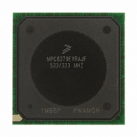
Manufacturer Part Number
MPC8379EVRAJF
Description
MPU PWRQUICC II 533MHZ 689TEPBGA
Manufacturer
Freescale Semiconductor
Series
PowerQUICC II PROr
Datasheets
1.MPC8377EVRAGD.pdf
(126 pages)
2.MPC8377EVRAGD.pdf
(2 pages)
3.MPC8379VRAGD.pdf
(116 pages)
Specifications of MPC8379EVRAJF
Processor Type
MPC83xx PowerQUICC II Pro 32-Bit
Speed
533MHz
Voltage
1V
Mounting Type
Surface Mount
Package / Case
689-TePBGA II
Maximum Clock Frequency
533 MHz
Operating Supply Voltage
1.8 V to 2.5 V
Maximum Operating Temperature
+ 105 C
Mounting Style
SMD/SMT
I/o Voltage
1.8 V, 2.5 V, 3.3 V
Minimum Operating Temperature
0 C
Core Size
32 Bit
Program Memory Size
64KB
Cpu Speed
533MHz
Embedded Interface Type
DUART, HSSI, I2C, IPIC, JTAG, SPI, USB
Digital Ic Case Style
BGA
No. Of Pins
689
Rohs Compliant
Yes
For Use With
MPC8377E-RDBA - BOARD REF DES MPC8377 REV 2.1MPC8377E-MDS-PB - BOARD MODULAR DEV SYSTEM
Lead Free Status / RoHS Status
Lead free / RoHS Compliant
Features
-
Lead Free Status / Rohs Status
Lead free / RoHS Compliant
Available stocks
Company
Part Number
Manufacturer
Quantity
Price
Company:

Part Number:
MPC8379EVRAJF
Manufacturer:
Freescale Semiconductor
Quantity:
135
Company:
Part Number:
MPC8379EVRAJF
Manufacturer:
Freescale Semiconductor
Quantity:
10 000


High-Speed Serial Interfaces (HSSI)
Figure 56
assumes that the DC levels of the clock driver chip is compatible with device SerDes reference clock
input’s DC requirement.
Figure 57
Since LVDS clock driver’s common-mode voltage is higher than the device SerDes reference clock input’s
allowed range (100 to 400 mV), AC-coupled connection scheme must be used. It assumes the LVDS
84
HCSL CLK Driver Chip
Total 50 Ω. Assume clock driver’s
output impedance is about 16 Ω.
Clock Driver
Clock Driver
Figure 56. DC-Coupled Differential Connection with HCSL Clock Driver (Reference Only)
shows the SerDes reference clock connection reference circuits for HCSL type clock driver. It
shows the SerDes reference clock connection reference circuits for LVDS type clock driver.
CLK_Out
CLK_Out
CLK_Out
Figure 56
fact that clock driver chip's internal structure, output impedance, and
termination requirements are different between various clock driver chip
manufacturers, it is very possible that the clock circuit reference designs
provided by the clock driver chip vendor are different from what is shown
below. They might also vary from one vendor to the other. Therefore,
Freescale Semiconductor can neither provide the optimal clock driver
reference circuits, nor guarantee the correctness of the following clock
driver connection reference circuits. The system designer is recommended
to contact the selected clock driver chip vendor for the optimal reference
circuits with the device SerDes reference clock receiver requirement
provided in this document.
MPC8377E PowerQUICC II Pro Processor Hardware Specifications, Rev. 4
to
33 Ω
33 Ω
Figure 59
Clock driver vendor dependent
source termination resistor
100 Ω differential PWB trace
below are for conceptual reference only. Due to the
NOTE
SDn_REF_CLK
SDn_REF_CLK
50 Ω
50 Ω
Freescale Semiconductor
MPC8377E
SerDes Refer.
CLK Receiver
Related parts for MPC8379EVRAJF
Image
Part Number
Description
Manufacturer
Datasheet
Request
R

Part Number:
Description:
BOARD REF DESIGN MPC8379E
Manufacturer:
Freescale Semiconductor
Datasheet:

Part Number:
Description:
BOARD REFERENCE FOR MPC837
Manufacturer:
Freescale Semiconductor
Datasheet:
Part Number:
Description:
BOARD PROCESSOR FOR MDS S
Manufacturer:
Freescale Semiconductor
Datasheet:

Part Number:
Description:
Powerquicc Ii Pro Processor Hardware Specifications
Manufacturer:
Freescale Semiconductor, Inc
Datasheet:

Part Number:
Description:
BOARD REF DES MPC8377 REV 2.1
Manufacturer:
Freescale Semiconductor
Datasheet:
Part Number:
Description:
Manufacturer:
Freescale Semiconductor, Inc
Datasheet:
Part Number:
Description:
Manufacturer:
Freescale Semiconductor, Inc
Datasheet:
Part Number:
Description:
Manufacturer:
Freescale Semiconductor, Inc
Datasheet:
Part Number:
Description:
Manufacturer:
Freescale Semiconductor, Inc
Datasheet:
Part Number:
Description:
Manufacturer:
Freescale Semiconductor, Inc
Datasheet:
Part Number:
Description:
Manufacturer:
Freescale Semiconductor, Inc
Datasheet:
Part Number:
Description:
Manufacturer:
Freescale Semiconductor, Inc
Datasheet:
Part Number:
Description:
Manufacturer:
Freescale Semiconductor, Inc
Datasheet:
Part Number:
Description:
Manufacturer:
Freescale Semiconductor, Inc
Datasheet:
Part Number:
Description:
Manufacturer:
Freescale Semiconductor, Inc
Datasheet: