604-00050 Parallax Inc, 604-00050 Datasheet
604-00050
Specifications of 604-00050


Related parts for 604-00050


604-00050 Summary of contents
Page 1
Introduction The uM-FPU V3.1 chip easily interfaces to virtually any 2 microcontroller using a SPI™ Many microcontrollers used in embedded systems lack floating point support, but a wide range of sensors available today require additional computations or data ...
Page 2
Features 32-bit Floating Point and 32-bit Integer A comprehensive set of 32-bit floating point and 32-bit integer operations are provided. See the uM-FPU V3.1 Instruction Set document for details. User-defined Functions User-defined functions can be stored in Flash and EEPROM. ...
Page 3
Block Diagram AVDD AVSS MCLR 12-bit Analog AN0 Power to Digital Control AN1 Converter uM-FPU EXTIN 32-bit Counter V3.1 Floating Point Coprocessor Instruction Buffer 256 bytes OSC1 OSC2 32-bit Floating Point 32-bit Long Integers Matrix Operations SPI™ Flash Memory CS ...
Page 4
Connecting to the uM-FPU V3.1 chip The uM-FPU V3.1 chip can be interfaced using one of several different types of SPI interface The different types are as follows: • 2-wire SPI interface, single device • 3-wire SPI ...
Page 5
SPI interface The 3-wire SPI connection uses separate data input and data output pins on the microcontroller. The CS pin is tied low to select SPI mode at Reset, and must remain low during operation. Microcontroller Pins DATA IN ...
Page 6
SPI Reset Operation The uM-FPU should be reset at the beginning of every program to ensure that the microcontroller and the uM-FPU are synchronized. The uM-FPU will prepare for a reset after nine consecutive 0xFF bytes are read, but it ...
Page 7
The OUT1 pin can also be used to check the Busy/Ready Status, see the section entitled Using OUT1 as a Ready/Busy Status. SPI Instruction Timing Diagrams SCLK SIN ...
Page 8
I C interface If the CS pin is a logic high at reset (e.g. tied to VDD), the uM-FPU will be configured interface allows the uM-FPU to share the I shown below. ...
Page 9
Slave Address S 1100100 S - Start Condition A - ACK N - NAK P - Stop Condition Register Address Item transfer speed Read Delay – normal operation Read Delay – debug enabled 2 ...
Page 10
On faster microcontrollers a suitable delay must be inserted after a read instruction to ensure that data is valid before the first byte is read. Using OUT1 as a Ready/Busy Status By default, the uM-FPU ...
Page 11
Debug Monitor The built-in Debug Monitor provides support for displaying the contents of uM-FPU registers, tracing the execution of uM-FPU instructions, setting breakpoints for debugging, and programming user functions. Whenever the uM- FPU V3.1 chip is reset and debug mode ...
Page 12
EEPROM – display EEPROM memory The EEPROM command displays the contents of the EEPROM memory in Intel Hex format. >E :1000000000000000000000000000000000000000F0 :1000100000000000000000000000000000000000E0 :100020000000000099000000000000000000000037 :1000300000000000000000000000000000000000C0 :100040000102030405060708090A0B0C0000000062 :1000500007360A33057F1680033301800000000055 :100060000000000000000000000000000000000090 :100070000000000000000000000000000000000080 :10008000FFFFFFFFFFFFFFFFFFFFFFFFFFFFFFFF80 :10009000FFFFFFFFFFFFFFFFFFFFFFFFFFFFFFFF70 . . . :1003D000FFFFFFFFFFFFFFFFFFFFFFFFFFFFFFFF2D :1003E000FFFFFFFFFFFFFFFFFFFFFFFFFFFFFFFF1D :1003F000FFFFFFFFFFFFFFFFFFFFFFFFFFFFFFFF0D Flash – display Flash ...
Page 13
Registers – display registers The Register command displays a header line showing the currently selected register A, register X, the internal status value, and if selected, matrix A, B and C. The current contents of all uM-FPU registers are then ...
Page 14
... F2" 0.00 000" 0101 5E 29 3602 3714 47 0102 2001 360A 53 61 97:03 0101 1F55 F2" 0.30902" 0101 5E 29 3604 3714 47 0102 2001 360A 53 61 97:06 0101 1F55 F2" 0.58779" 0101 5E 29 3606 3714 47 0102 2001 360A 53 61 97:08 0101 1 F55 F2" ...
Page 15
Clock – select clock source The Clock command allows you to change the clock source. The default clock speed is 29.48 MHz using an internal oscillator which provides the maximum execution speed. The clock speed would only need to be ...
Page 16
Mode – set mode parameters The Mode command is used to set the four interface mode parameter bytes that are stored in Flash memory. The factory setting of the parameter bytes is all zeros. The parameter bytes are read at ...
Page 17
Program – program user function memory The Program command is used to program the user function memory. Once in program mode, the uM-FPU looks for valid Intel Hex format records. The records must have an address between 0x0000 and 0x03C0, ...
Page 18
Debug Instructions There are several instructions that are designed to work in conjunction with the debug monitor. If the debug monitor is not enabled, these commands are NOPs. The instructions are as follows: BREAK When the BREAK instruction is encountered, ...
Page 19
Flash Memory There are 2304 bytes of Flash memory reserved on the uM-FPU for storing user-defined functions and the mode parameters user-defined functions can be stored in Flash memory. User-defined functions have the advantage of conserving space ...
Page 20
EEPROM Memory There are 1024 bytes of EEPROM memory reserved on the uM-FPU for storing user-defined functions and data. The EESAVE, EESAVEA, EELOAD, EELOADA instructions are used to store and retrieve data. The EEWRITE instruction is used to store user-defined ...
Page 21
PDIP-18 Through-Hole Package Micromega Corporation 21 uM-FPU V3.1 Datasheet ...
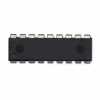
Page 22
SOIC-18 Surface Mount Package Micromega Corporation 22 uM-FPU V3.1 Datasheet ...
Page 23
QFN-44 Surface Mount Package Micromega Corporation 23 uM-FPU V3.1 Datasheet ...
Page 24
Absolute Maximum Ratings Parameter Storage Temperature Ambient Temperature with Power Applied Supply Voltage on VDD relative to VSS Input Voltage relative to VSS Maximum Current out of VSS pin Maximum Current into VDD pin Maximum Current sourced by any I/O ...
Page 25
Appendix A uM-FPU V3.1 Instruction Summary Instruction Opcode Arguments NOP 00 SELECTA 01 nn SELECTX 02 nn CLR 03 nn CLRA 04 CLRX 05 CLR0 06 COPY 07 mm,nn COPYA 08 nn COPYX 09 nn LOAD 0A nn LOADA 0B ...
Page 26
FSUBR0 2C FMUL0 2D FDIV0 2E FDIVR0 2F FPOW0 30 FCMP0 31 FSETI 32 bb FADDI 33 bb FSUBI 34 bb FSUBRI 35 bb FMULI 36 bb FDIVI 37 bb FDIVRI 38 bb FPOWI 39 bb FCMPI 3A bb FSTATUS ...
Page 27
LOADUBYTE 5A bb LOADWORD 5B b1,b2 LOADUWORD 5C b1,b2 LOADE 5D LOADPI 5E LOADCON 5F bb FLOAT 60 FIX 61 FIXR 62 FRAC 63 FSPLIT 64 SELECTMA 65 nn,bb,bb SELECTMB 66 nn,bb,bb SELECTMC 67 nn,bb,bb LOADMA 68 bb,bb LOADMB 69 ...
Page 28
LREADA 95 LREADX 96 LREAD0 97 LREADBYTE 98 LREADWORD 99 ATOL 9A aa…00 LTOA 9B bb LSET 9C nn LADD 9D nn LSUB 9E nn LMUL 9F nn LDIV A0 nn LCMP A1 nn LUDIV A2 nn LUCMP A3 nn ...
Page 29
LSTATUS B7 nn LSTATUSA B8 LCMP2 B9 nn,mm LUCMP2 BA nn,mm LNEG BB LABS BC LINC BD nn LDEC BE nn LNOT BF LAND C0 nn LOR C1 nn LXOR C2 nn LSHIFT C3 nn LMIN C4 nn LMAX C5 ...
Page 30
STRFIND E7 aa…00 STRFCHR E8 aa…00 STRFIELD E9 bb STRTOF EA STRTOL EB READSEL EC STRBYTE ED bb STRINC EE STRDEC EF SYNC F0 READSTATUS F1 READSTR F2 VERSION F3 IEEEMODE F4 PICMODE F5 CHECKSUM F6 BREAK F7 TRACEOFF F8 ...
Page 31
Appendix B uM-FPU V3.1 Instruction Timing The instruction times shown in the following table are calculated with a clock speed of 29.48 MHz and are measured from the rising edge of the last bit of the last byte of the ...
Page 32
FREADX 1C FREAD0 1D ATOF 1E aa…00 FTOA 1F bb FSET 20 nn FADD 21 nn FSUB 22 nn FSUBR 23 nn FMUL 24 nn FDIV 25 nn FDIVR 26 nn FPOW 27 nn FCMP 28 nn FSET0 29 FADD0 ...
Page 33
ATAN2 4D nn DEGREES 4E RADIANS 4F FMOD 50 nn FLOOR 51 CEIL 52 ROUND 53 FMIN 54 nn FMAX 55 nn FCNV 56 bb FMAC 57 nn,mm FMSC 58 nn,mm LOADBYTE 59 bb LOADUBYTE 5A bb LOADWORD 5B b1,b2 ...
Page 34
FTABLE 86 cc,tc,t1…tn LTABLE 87 cc,tc,t1…tn POLY 88 tc,t1…tn GOTO 89 nn RET, LWRITE 90 nn,b1,b2,b3,b4 LWRITEA 91 b1,b2,b3,b4 LWRITEX 92 b1,b2,b3,b4 LWRITE0 93 b1,b2,b3,b4 LREAD 94 nn LREADA 95 LREADX 96 LREAD0 97 LREADBYTE 98 LREADWORD 99 ...
Page 35
LABS BC LINC BD nn LDEC BE nn LNOT BF LAND C0 nn LOR C1 nn LXOR C2 nn LSHIFT C3 nn LMIN C4 nn LMAX C5 nn LONGBYTE C6 bb LONGUBYTE C7 bb LONGWORD C8 b1,b2 LONGUWORD C9 b1,b2 ...
Page 36
STRDEC EF SYNC F0 READSTATUS F1 READSTR F2 VERSION F3 IEEEMODE F4 PICMODE F5 CHECKSUM F6 BREAK F7 TRACEOFF F8 TRACEON F9 TRACESTR FA aa…00 TRACEREG FB nn READVAR FC bb RESET FF Notes: 1. The minimum Read Setup Delay ...