604-00050 Parallax Inc, 604-00050 Datasheet - Page 6
604-00050
Manufacturer Part Number
604-00050
Description
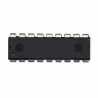
IC FLOATING-PT COPROC V3 18-DIP
Manufacturer
Parallax Inc
Datasheet
1.604-00050.pdf
(36 pages)
Specifications of 604-00050
Processor Type
Floating-Point Co-Processor
Voltage
2.7V ~ 5.5V
Mounting Type
Through Hole
Package / Case
*
Lead Free Status / RoHS Status
Lead free / RoHS Compliant
Features
-
Speed
-
Lead Free Status / RoHS Status
Lead free / RoHS Compliant, Lead free / RoHS Compliant


SPI Reset Operation
The uM-FPU should be reset at the beginning of every program to ensure that the microcontroller and the uM-FPU
are synchronized. The uM-FPU will prepare for a reset after nine consecutive 0xFF bytes are read, but it is
recommended that ten 0xFF bytes be sent by the microcontroller to ensure that at least nine 0xFF bytes are
recognized even if the microcontroller and uM-FPU are out of sync. The reset does not occur until the SIN signal
goes Low. If SIN remains High after sending the ten 0xFF bytes, a 0x00 byte must be sent (or SIN set Low) to
trigger the reset. Note: If SIN does not go Low within 100 milliseconds of receiving nine 0xFF bytes, a reset will be
triggered by default. A delay of 10 milliseconds is recommended after the reset is triggered to ensure that the reset
sequence is complete and the uM-FPU is ready to receive commands. All uM-FPU registers are reset to the special
value NaN (Not a Number), which is equal to hexadecimal 7FFFFFFF.
SPI Reading and Writing Data
The uM-FPU is configured as a Serial Peripheral Interconnect (SPI) slave device. Data is transmitted and received
with the most significant bit (MSB) first using SPI mode 0, summarized as follows:
The maximum SCLK frequency is 15 MHz, but there must be minimum data period between bytes. The minimum
data period is measured from the rising edge of the first bit of one date byte to the rising edge of the first bit of the
next data byte. The minimum data period must elapse before the Busy/Ready status is checked.
Read Delay
There is a minimum delay (Read Setup Delay) required from the end of a read instruction opcode until the first data
byte is ready to be read. With many microcontrollers the call overhead for the interface routines is long enough that
no additional delay is required. On faster microcontrollers a suitable delay must be inserted after a read instruction to
ensure that data is valid before the first byte is read.
SPI Busy/Ready Status
The busy/ready status must always be checked to confirm the Ready status prior to any read operation.
The Busy status is asserted as soon as an instruction byte is received. The Ready status is asserted when both the
instruction buffer and trace buffer are empty. If the uM-FPU is Ready the SOUT pin is held Low. If the uM-FPU is
Busy, either executing instructions, or because the debug monitor is active, the SOUT pin is held High. The
minimum data period must have elapsed since the last byte was transmitted before the SOUT status is checked. If
more than 256 bytes of data are sent between read operations, the Ready status must also be checked at least once
Micromega Corporation
SCLK
SCLK is active High (idle state is Low)
Data latched on leading edge of SCLK
Data changes on trailing edge of SCLK
Data is transmitted most significant bit first
SIN
Item
Reset - 0xFF bytes
Reset - SIN Low
Reset Delay
9 - 0xFF bytes
Reset Timing Diagram
6
Min
10
9
SIN Low
Typical
10
Reset
Delay
Connecting to the uM-FPU V3.1
Max
100
uM-FPU V3.1 Datasheet
bytes
msec
msec
Unit
Related parts for 604-00050
Image
Part Number
Description
Manufacturer
Datasheet
Request
R

Part Number:
Description:
IC ADC 12BIT 8CH MAX1270 24-DIP
Manufacturer:
Parallax Inc
Datasheet:

Part Number:
Description:
IC EMBEDDED USB HOST 48-LQFP
Manufacturer:
Parallax Inc
Datasheet:

Part Number:
Description:
IC SENSOR TOUCH/PROXMTY 1CH 8DIP
Manufacturer:
Parallax Inc
Datasheet:

Part Number:
Description:
IC FLOATING-POINT COPROC V2 8DIP
Manufacturer:
Parallax Inc
Datasheet:


Part Number:
Description:
Microcontroller Modules & Accessories DISCONTINUED BY PARALLAX
Manufacturer:
Parallax Inc

Part Number:
Description:
BOOK UNDERSTANDING SIGNALS
Manufacturer:
Parallax Inc
Datasheet:


Part Number:
Description:
COMPETITION RING FOR SUMOBOT
Manufacturer:
Parallax Inc
Datasheet:


Part Number:
Description:
TEXT INFRARED REMOTE FOR BOE-BOT
Manufacturer:
Parallax Inc
Datasheet:
Part Number:
Description:
BOARD EXPERIMENT+LCD NX-1000
Manufacturer:
Parallax Inc
Datasheet:

Part Number:
Description:
CONTROLLER 16SERVO MOTOR CONTROL
Manufacturer:
Parallax Inc
Datasheet: