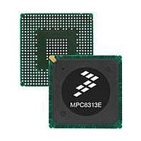
MPC8313VRADDB Freescale Semiconductor, MPC8313VRADDB Datasheet - Page 16

MPC8313VRADDB
Manufacturer Part Number
MPC8313VRADDB
Description
MPU POWERQUICC II PRO 516-PBGA
Manufacturer
Freescale Semiconductor
Datasheet
1.MPC8313CZQAFFB.pdf
(100 pages)
Specifications of MPC8313VRADDB
Processor Type
MPC83xx PowerQUICC II Pro 32-Bit
Speed
267MHz
Voltage
0.95 V ~ 1.05 V
Mounting Type
Surface Mount
Package / Case
516-PBGA
Processor Series
MPC8xxx
Core
e300
Data Bus Width
32 bit
Development Tools By Supplier
MPC8313E-RDB
Maximum Clock Frequency
400 MHz
Operating Supply Voltage
- 0.3 V to + 1.26 V
Maximum Operating Temperature
+ 105 C
Mounting Style
SMD/SMT
Data Ram Size
16 KB
I/o Voltage
2.5 V
Interface Type
I2C, SPI, UART
Minimum Operating Temperature
- 40 C
Program Memory Type
EEPROM/Flash
Lead Free Status / RoHS Status
Lead free / RoHS Compliant
Features
-
Lead Free Status / Rohs Status
Lead free / RoHS Compliant
Available stocks
Company
Part Number
Manufacturer
Quantity
Price
Company:
Part Number:
MPC8313VRADDB
Manufacturer:
MOTOLOLA
Quantity:
885
Company:
Part Number:
MPC8313VRADDB
Manufacturer:
Freescale Semiconductor
Quantity:
10 000
DDR and DDR2 SDRAM
Table 16
6.2
This section provides the AC electrical characteristics for the DDR SDRAM interface.
6.2.1
Table 17
Table 18
Table 19
16
At recommended operating conditions with GV
At recommended operating conditions with GV
At recommended operating conditions. with GV
Current draw for MV
Note:
1. The voltage regulator for MV
AC input low voltage
AC input high voltage
AC input low voltage
AC input high voltage
Controller skew for MDQS—MDQ
333 MHz
266 MHz
Notes:
1. t
2. The amount of skew that can be tolerated from MDQS to a corresponding MDQ signal is called t
is captured with MDQS[ n ]. This should be subtracted from the total timing budget.
determined by the following equation: t
absolute value of t
CISKEW
provides the current draw characteristics for MV
provides the input AC timing specifications for the DDR2 SDRAM when
provides the input AC timing specifications for the DDR SDRAM when GV
provides the input AC timing specifications for the DDR2 SDRAM interface.
represents the total amount of skew consumed by the controller between MDQS[ n ] and any corresponding bit that
DDR and DDR2 SDRAM AC Electrical Characteristics
Parameter/Condition
DDR and DDR2 SDRAM Input AC Timing Specifications
Parameter
Parameter
Table 17. DDR2 SDRAM Input AC Timing Specifications for 1.8-V Interface
Parameter
Table 18. DDR SDRAM Input AC Timing Specifications for 2.5-V Interface
REF
CISKEW
MPC8313E PowerQUICC
Table 19. DDR and DDR2 SDRAM Input AC Timing Specifications
.
REF
Table 16. Current Draw Characteristics for MV
must be able to supply up to 500 μA current.
DD
DD
DISKEW
DD
of 1.8 ± 5%.
of 2.5 ± 5%.
of 2.5 ± 5%.
Symbol
Symbol
™
= ± (T/4 – abs(t
V
V
V
V
II Pro Processor Hardware Specifications, Rev. 3
IH
IH
IL
IL
Symbol
Symbol
t
I
CISKEW
MVREF
—
—
CISKEW
MV
MV
REF
REF
REF
Min
Min
—
—
)) where T is the clock period and abs(t
+ 0.25
+ 0.31
.
–750
–750
Min
Min
—
—
MV
MV
REF
REF
REF
Max
Max
—
—
Max
Max
500
750
750
– 0.25
– 0.31
—
DISKEW
GV
Freescale Semiconductor
DD
DD
. This can be
(typ) = 2.5 V.
(typ) =
Unit
Unit
Unit
Unit
μA
ps
—
—
V
V
V
V
CISKEW
1.8 V.
Notes
Notes
Notes
) is the
Note
1, 2
—
—
—
—
—
—
1


