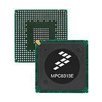
MPC8313VRADDB Freescale Semiconductor, MPC8313VRADDB Datasheet - Page 31

MPC8313VRADDB
Manufacturer Part Number
MPC8313VRADDB
Description
MPU POWERQUICC II PRO 516-PBGA
Manufacturer
Freescale Semiconductor
Datasheet
1.MPC8313CZQAFFB.pdf
(100 pages)
Specifications of MPC8313VRADDB
Processor Type
MPC83xx PowerQUICC II Pro 32-Bit
Speed
267MHz
Voltage
0.95 V ~ 1.05 V
Mounting Type
Surface Mount
Package / Case
516-PBGA
Processor Series
MPC8xxx
Core
e300
Data Bus Width
32 bit
Development Tools By Supplier
MPC8313E-RDB
Maximum Clock Frequency
400 MHz
Operating Supply Voltage
- 0.3 V to + 1.26 V
Maximum Operating Temperature
+ 105 C
Mounting Style
SMD/SMT
Data Ram Size
16 KB
I/o Voltage
2.5 V
Interface Type
I2C, SPI, UART
Minimum Operating Temperature
- 40 C
Program Memory Type
EEPROM/Flash
Lead Free Status / RoHS Status
Lead free / RoHS Compliant
Features
-
Lead Free Status / Rohs Status
Lead free / RoHS Compliant
Available stocks
Company
Part Number
Manufacturer
Quantity
Price
Company:
Part Number:
MPC8313VRADDB
Manufacturer:
MOTOLOLA
Quantity:
885
Company:
Part Number:
MPC8313VRADDB
Manufacturer:
Freescale Semiconductor
Quantity:
10 000
8.3.4.1
Table 34
8.3.4.2
Table 35
supported. Clock is recovered from the data.
eye diagram.
Freescale Semiconductor
At recommended operating conditions with XCOREV
At recommended operating conditions with XCOREV
Deterministic jitter
Total jitter
Unit interval
V
V
Note:
1. Each UI is 800 ps ± 100 ppm.
Deterministic jitter tolerance
Combined deterministic and random jitter tolerance
Sinusoidal jitter tolerance
Total jitter tolerance
Bit error ratio
Unit interval
AC coupling capacitor
Notes:
1. Measured at receiver.
2. Each UI is 800 ps ± 100 ppm.
3. The external AC coupling capacitor is required. It is recommended to be placed near the device transmitter outputs.
4. Refer to the RapidIO™ 1x/4x LP Serial Physical Layer Specification , for interpretation of jitter specifications.
OD
OD
fall time (80%–20%)
rise time (20%–80%)
provides the SGMII transmit AC timing targets. A source synchronous clock is not provided.
provides the SGMII receive AC timing specifications. Source synchronous clocking is not
SGMII Transmit AC Timing Specifications
SGMII Receive AC Timing Specifications
Parameter
Parameter
MPC8313E PowerQUICC
Table 34. SGMII Transmit AC Timing Specifications
Table 35. SGMII Receive AC Timing Specifications
DD
DD
™
Symbol
= 1.0 V ± 5%.
= 1.0 V ± 5%.
II Pro Processor Hardware Specifications, Rev. 3
tfall
t
JD
JT
UI
rise
Figure 17
Symbol
JSIN
BER
JDR
C
JD
JT
UI
TX
799.92
shows the SGMII receiver input compliance mask
Min
50
50
—
—
799.92
0.37
0.55
0.65
Min
0.1
—
5
Ethernet: Three-Speed Ethernet, MII Management
Typ
800
—
—
—
—
Typ
800
—
—
—
—
—
—
800.08
800.08
Max
0.17
0.35
120
120
10
Max
200
—
—
—
—
–12
UI p-p
UI p-p
UI p-p
UI p-p
UI p-p
UI p-p
Unit
Unit
nF
ps
ps
ps
ps
Notes
Notes
1
1
1
1
3
1
2
31


