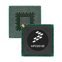
MPC8313VRADDB Freescale Semiconductor, MPC8313VRADDB Datasheet - Page 36

MPC8313VRADDB
Manufacturer Part Number
MPC8313VRADDB
Description
MPU POWERQUICC II PRO 516-PBGA
Manufacturer
Freescale Semiconductor
Datasheet
1.MPC8313CZQAFFB.pdf
(100 pages)
Specifications of MPC8313VRADDB
Processor Type
MPC83xx PowerQUICC II Pro 32-Bit
Speed
267MHz
Voltage
0.95 V ~ 1.05 V
Mounting Type
Surface Mount
Package / Case
516-PBGA
Processor Series
MPC8xxx
Core
e300
Data Bus Width
32 bit
Development Tools By Supplier
MPC8313E-RDB
Maximum Clock Frequency
400 MHz
Operating Supply Voltage
- 0.3 V to + 1.26 V
Maximum Operating Temperature
+ 105 C
Mounting Style
SMD/SMT
Data Ram Size
16 KB
I/o Voltage
2.5 V
Interface Type
I2C, SPI, UART
Minimum Operating Temperature
- 40 C
Program Memory Type
EEPROM/Flash
Lead Free Status / RoHS Status
Lead free / RoHS Compliant
Features
-
Lead Free Status / Rohs Status
Lead free / RoHS Compliant
Available stocks
Company
Part Number
Manufacturer
Quantity
Price
Company:
Part Number:
MPC8313VRADDB
Manufacturer:
MOTOLOLA
Quantity:
885
Company:
Part Number:
MPC8313VRADDB
Manufacturer:
Freescale Semiconductor
Quantity:
10 000
High-Speed Serial Interfaces (HSSI)
Figure 21
9
This section describes the common portion of SerDes DC electrical specifications, which is the DC
requirement for SerDes reference clocks. The SerDes data lane’s transmitter and receiver reference circuits
are also shown.
9.1
The SerDes utilizes differential signaling to transfer data across the serial link. This section defines terms
used in the description and specification of differential signals.
Figure 22
description. The figure shows waveform for either a transmitter output (TXn and TXn) or a receiver input
(RXn and RXn). Each signal swings between A volts and B volts where A > B.
Using this waveform, the definitions are as follows. To simplify illustration, the following definitions
assume that the SerDes transmitter and receiver operate in a fully symmetrical differential signaling
environment.
36
1. Single-ended swing
2. Differential output voltage, V
3. Differential input voltage, V
High-Speed Serial Interfaces (HSSI)
The transmitter output signals and the receiver input signals TXn, TXn, RXn, and RXn each have
a peak-to-peak swing of A – B volts. This is also referred as each signal wire’s single-ended swing.
The differential output voltage (or swing) of the transmitter, V
the two complimentary output voltages: V
negative.
The differential input voltage (or swing) of the receiver, V
complimentary input voltages: V
Signal Terms Definition
shows the MII management AC timing diagram.
shows how the signals are defined. For illustration purpose, only one SerDes lane is used for
(Output)
(Input)
MDIO
MDIO
MPC8313E PowerQUICC
MDC
Figure 21. MII Management Interface Timing Diagram
t
MDCH
ID
t
MDDVKH
OD
t
(or differential input swing):
MDC
RXn
(or differential output swing):
™
t
MDKHDX
II Pro Processor Hardware Specifications, Rev. 3
– V
RXn
TXn
. The V
t
– V
MDCF
TXn.
ID
t
MDDXKH
The V
value can be either positive or negative.
t
ID
MDCR
, is defined as the difference of the two
OD
OD
value can be either positive or
, is defined as the difference of
Freescale Semiconductor


