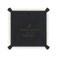
MC68020EH16E Freescale Semiconductor, MC68020EH16E Datasheet - Page 51

MC68020EH16E
Manufacturer Part Number
MC68020EH16E
Description
IC MPU 32BIT 33MHZ 132-PQFP
Manufacturer
Freescale Semiconductor
Datasheet
1.MC68020EH16E.pdf
(306 pages)
Specifications of MC68020EH16E
Processor Type
M680x0 32-Bit
Speed
166MHz
Voltage
5V
Mounting Type
Surface Mount
Package / Case
132-MQFP, 132-PQFP
Family Name
M68000
Device Core
ColdFire
Device Core Size
32b
Frequency (max)
16.67MHz
Instruction Set Architecture
RISC
Supply Voltage 1 (typ)
5V
Operating Supply Voltage (max)
5.25V
Operating Supply Voltage (min)
4.75V
Operating Temp Range
0C to 70C
Operating Temperature Classification
Commercial
Mounting
Surface Mount
Pin Count
132
Package Type
PQFP
Lead Free Status / RoHS Status
Lead free / RoHS Compliant
Features
-
Lead Free Status / Rohs Status
Compliant
Available stocks
Company
Part Number
Manufacturer
Quantity
Price
Company:
Part Number:
MC68020EH16E
Manufacturer:
Freescale Semiconductor
Quantity:
10 000
- Current page: 51 of 306
- Download datasheet (3Mb)
Freescale Semiconductor, Inc.
a write cycle, all 32 bits of the data bus are driven, regardless of the port width or operand
size. The processor places the data on the data bus one-half clock cycle after A S is
asserted in a write cycle.
5.1.5 Data Strobe
DS is a timing signal that applies to the data bus. For a read cycle, the processor asserts
DS to signal the external device to place data on the bus. DS is asserted at the same time
as AS during a read cycle. For a write cycle, DS notifies the external device that the data
to be written is valid. The processor asserts DS one full clock cycle after the assertion of
AS during a write cycle.
5.1.6 Data Buffer Enable
The MC68020 DBEN signal is used to enable external data buffers while data is present
on the data bus. During a read operation, DBEN is asserted one clock cycle after the
beginning of the bus cycle and is negated as DS is negated. In a write operation, DBEN is
asserted at the time AS is asserted and is held active for the duration of the cycle. Note
that DBEN is implemented in the MC68020 and is not implemented in the MC68EC020.
5.1.7 Bus Cycle Termination Signals
During bus cycles, external devices assert DSACK1/DSACK0 as part of the bus protocol.
During a read cycle, DSACK1/DSACK0 assertion signals the processor to terminate the
bus cycle and to latch the data. During a write cycle, the assertion of DSACK1/DSACK0
indicates that the external device has successfully stored the data and that the cycle may
terminate. DSACK1/DSACK0 also indicate to the processor the size of the port for the bus
cycle just completed, as shown in Table 5-1. Refer to 5.3.1 Read Cycle for timing
relationships of DSACK1/DSACK0.
The BERR signal is also a bus cycle termination indicator and can be used in the absence
of DSACK1/DSACK0 to indicate a bus error condition. It can also be asserted in
conjunction with DSACK1/DSACK0 to indicate a bus error condition, provided it meets the
appropriate timing described in this section and in Section 10 Electrical Characteristics.
Additionally, the BERR and HALT signals can be asserted together to indicate a retry
termination. Again, the BERR and HALT signals can be simultaneously asserted in lieu of,
or in conjunction with, the DSACK1/DSACK0 signals.
Finally, the AVEC signal can be used to terminate interrupt acknowledge cycles, indicating
that the MC68020/EC020 should generate a vector number to locate an interrupt handler
routine. AVEC is ignored during all other bus cycles.
5-4
M68020 USER’S MANUAL
MOTOROLA
For More Information On This Product,
Go to: www.freescale.com
Related parts for MC68020EH16E
Image
Part Number
Description
Manufacturer
Datasheet
Request
R

Part Number:
Description:
(MC600 Series) INTEGRATED CIRCUITS
Manufacturer:
ETC
Datasheet:
Part Number:
Description:
Manufacturer:
Freescale Semiconductor, Inc
Datasheet:
Part Number:
Description:
Manufacturer:
Freescale Semiconductor, Inc
Datasheet:
Part Number:
Description:
Manufacturer:
Freescale Semiconductor, Inc
Datasheet:
Part Number:
Description:
Manufacturer:
Freescale Semiconductor, Inc
Datasheet:
Part Number:
Description:
Manufacturer:
Freescale Semiconductor, Inc
Datasheet:
Part Number:
Description:
Manufacturer:
Freescale Semiconductor, Inc
Datasheet:
Part Number:
Description:
Manufacturer:
Freescale Semiconductor, Inc
Datasheet:
Part Number:
Description:
Manufacturer:
Freescale Semiconductor, Inc
Datasheet:
Part Number:
Description:
Manufacturer:
Freescale Semiconductor, Inc
Datasheet:
Part Number:
Description:
Manufacturer:
Freescale Semiconductor, Inc
Datasheet:
Part Number:
Description:
Manufacturer:
Freescale Semiconductor, Inc
Datasheet:
Part Number:
Description:
Manufacturer:
Freescale Semiconductor, Inc
Datasheet:
Part Number:
Description:
Manufacturer:
Freescale Semiconductor, Inc
Datasheet:
Part Number:
Description:
Manufacturer:
Freescale Semiconductor, Inc
Datasheet:


