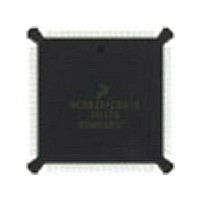
MC68020EH16E Freescale Semiconductor, MC68020EH16E Datasheet - Page 72

MC68020EH16E
Manufacturer Part Number
MC68020EH16E
Description
IC MPU 32BIT 33MHZ 132-PQFP
Manufacturer
Freescale Semiconductor
Datasheet
1.MC68020EH16E.pdf
(306 pages)
Specifications of MC68020EH16E
Processor Type
M680x0 32-Bit
Speed
166MHz
Voltage
5V
Mounting Type
Surface Mount
Package / Case
132-MQFP, 132-PQFP
Family Name
M68000
Device Core
ColdFire
Device Core Size
32b
Frequency (max)
16.67MHz
Instruction Set Architecture
RISC
Supply Voltage 1 (typ)
5V
Operating Supply Voltage (max)
5.25V
Operating Supply Voltage (min)
4.75V
Operating Temp Range
0C to 70C
Operating Temperature Classification
Commercial
Mounting
Surface Mount
Pin Count
132
Package Type
PQFP
Lead Free Status / RoHS Status
Lead free / RoHS Compliant
Features
-
Lead Free Status / Rohs Status
Compliant
Available stocks
Company
Part Number
Manufacturer
Quantity
Price
Company:
Part Number:
MC68020EH16E
Manufacturer:
Freescale Semiconductor
Quantity:
10 000
- Current page: 72 of 306
- Download datasheet (3Mb)
for asynchronous operation can be ignored. All timing parameters referred to are
described in Section 10 Electrical Characteristics. If a system asserts
DSACK1/DSACK0 for the required window around the falling edge of state 2 and obeys
the proper bus protocol by maintaining DSACK1/DSACK0 (and/or BERR/HALT) until and
throughout the clock edge that negates AS (with the appropriate asynchronous input hold
time specified by parameter #47B), no wait states are inserted. The bus cycle runs at its
maximum speed of three clocks per cycle for bus cycles terminated with
DSACK1/DSACK0.
To ensure proper operation in a synchronous system when BERR or BERR/HALT is
asserted after DSACK1/DSACK0, BERR (and HALT) must meet the appropriate setup time
(parameter #27A) prior to the falling clock edge one clock cycle after DSACK1/DSACK0 is
recognized. This setup time is critical, and the MC68020/EC020 may exhibit erratic
behavior if it is violated.
When operating synchronously, the data-in setup (parameter #27) and hold (parameter
#30) times for synchronous cycles may be used instead of the timing requirements for
data relative to the DS signal.
5.3 DATA TRANSFER CYCLES
The transfer of data between the processor and other devices involves the following
signals:
The address and data buses are both parallel, nonmultiplexed buses. The bus master
moves data on the bus by issuing control signals, and the bus uses a handshake protocol
to ensure correct movement of the data. In all bus cycles, the bus master is responsible
for de-skewing all signals it issues at both the start and end of the cycle. In addition, the
bus master is responsible for de-skewing DSACK1/DSACK0, D31–D0, BERR, HALT, and,
for the MC68020, DBEN from the slave devices. The following paragraphs define read,
write, and read-modify-write cycle operations.
Each of the bus cycles is defined as a succession of states. These states apply to the bus
operation and are different from the processor states described in Section 2 Processing
States. The clock cycles used in the descriptions and timing diagrams of data transfer
cycles are independent of the clock frequency. Bus operations are described in terms of
external bus states.
MOTOROLA
• Address Bus (A31–A0 for the MC68020) (A23–A0 for the MC68EC020)
• Data Bus (D31–D0)
• Control Signals
Freescale Semiconductor, Inc.
For More Information On This Product,
Go to: www.freescale.com
M68020 USER’S MANUAL
5- 25
Related parts for MC68020EH16E
Image
Part Number
Description
Manufacturer
Datasheet
Request
R

Part Number:
Description:
(MC600 Series) INTEGRATED CIRCUITS
Manufacturer:
ETC
Datasheet:
Part Number:
Description:
Manufacturer:
Freescale Semiconductor, Inc
Datasheet:
Part Number:
Description:
Manufacturer:
Freescale Semiconductor, Inc
Datasheet:
Part Number:
Description:
Manufacturer:
Freescale Semiconductor, Inc
Datasheet:
Part Number:
Description:
Manufacturer:
Freescale Semiconductor, Inc
Datasheet:
Part Number:
Description:
Manufacturer:
Freescale Semiconductor, Inc
Datasheet:
Part Number:
Description:
Manufacturer:
Freescale Semiconductor, Inc
Datasheet:
Part Number:
Description:
Manufacturer:
Freescale Semiconductor, Inc
Datasheet:
Part Number:
Description:
Manufacturer:
Freescale Semiconductor, Inc
Datasheet:
Part Number:
Description:
Manufacturer:
Freescale Semiconductor, Inc
Datasheet:
Part Number:
Description:
Manufacturer:
Freescale Semiconductor, Inc
Datasheet:
Part Number:
Description:
Manufacturer:
Freescale Semiconductor, Inc
Datasheet:
Part Number:
Description:
Manufacturer:
Freescale Semiconductor, Inc
Datasheet:
Part Number:
Description:
Manufacturer:
Freescale Semiconductor, Inc
Datasheet:
Part Number:
Description:
Manufacturer:
Freescale Semiconductor, Inc
Datasheet:


