LE80538VE0041M Intel, LE80538VE0041M Datasheet - Page 18
LE80538VE0041M
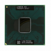
Manufacturer Part Number
LE80538VE0041M
Description
IC PROC CELERON M 1.06GHZ 479BGA
Manufacturer
Intel
Datasheet
1.LE80535NC013512.pdf
(69 pages)
Specifications of LE80538VE0041M
Processor Type
Celeron M
Features
533MHZ Bus, 1M L2 Cache
Speed
1.06GHz
Voltage
0.94V
Mounting Type
Surface Mount
Package / Case
479-BGA
Lead Free Status / RoHS Status
Lead free / RoHS Compliant
Other names
883549
Available stocks
Company
Part Number
Manufacturer
Quantity
Price


Electrical Specifications
3.6
3.7
18
Signal Terminations and Unused Pins
All RSVD (RESERVED) pins must remain unconnected. Connection of these pins to V
to any other signal (including each other) can result in component malfunction or incompatibility
with future Intel Celeron M processors. See
location of all RSVD pins.
For reliable operation, always connect unused inputs or bidirectional signals to an appropriate
signal level. Unused active low AGTL+ inputs may be left as no connects if AGTL+ termination is
provided on the processor silicon. Unused active high inputs should be connected through a resistor
to ground (V
For details on signal terminations, please refer to the platform design guides. TAP signal
termination requirements are also discussed in ITP700 Debug Port Design Guide .
The TEST1, TEST2, and TEST3 pins must be left unconnected but should have a stuffing option
connection to V
FSB Signal Groups
In order to simplify the following discussion, the FSB signals have been combined into groups by
buffer type. AGTL+ input signals have differential input buffers, which use GTLREF as a reference
level. In this document, the term "AGTL+ Input" refers to the AGTL+ input group as well as the
AGTL+ I/O group when receiving. Similarly, "AGTL+ Output" refers to the AGTL+ output group
as well as the AGTL+ I/O group when driving.
With the implementation of a source synchronous data bus comes the need to specify two sets of
timing parameters. One set is for common clock signals which are dependant upon the crossing of
the rising edge of BCLK0 and the falling edge of BCLK1. The second set is for the source
synchronous signals which are relative to their respective strobe lines (data and address) as well as
the rising edge of BCLK0. Asychronous signals are still present (A20M#, IGNNE#, etc.) and can
become active at any time during the clock cycle.
clock, source synchronous, and asynchronous.
SS
). Unused outputs can be left unconnected.
SS
separately via 1-k Ω, pull-down resistors.
Section 4.1
Table 3
for a pin listing of the processor and the
identifies which signals are common
Intel
®
Celeron
®
M Processor Datasheet
CC
, V
SS
, or
Related parts for LE80538VE0041M
Image
Part Number
Description
Manufacturer
Datasheet
Request
R

Part Number:
Description:
Microprocessor: Intel Celeron M Processor 320 and Ultra Low Voltage Intel Celeron M Processor at 600MHz
Manufacturer:
Intel Corporation
Part Number:
Description:
Intel 82550 Fast Ethernet Multifunction PCI/CardBus Controller
Manufacturer:
Intel Corporation
Datasheet:
Part Number:
Description:
Intel StrataFlash memory 32 Mbit. Access speed 120 ns
Manufacturer:
Intel Corporation
Datasheet:
Part Number:
Description:
Intel StrataFlash memory 32 Mbit. Access speed 120 ns
Manufacturer:
Intel Corporation
Datasheet:
Part Number:
Description:
Intel StrataFlash memory 64 Mbit. Access speed 150 ns
Manufacturer:
Intel Corporation
Datasheet:
Part Number:
Description:
Intel StrataFlash memory 32 Mbit. Access speed 100 ns
Manufacturer:
Intel Corporation
Datasheet:
Part Number:
Description:
DA28F640J5A-1505 Volt Intel StrataFlash Memory
Manufacturer:
Intel Corporation
Datasheet:
Part Number:
Description:
5 Volt Intel StrataFlash?? Memory
Manufacturer:
Intel Corporation
Datasheet:
Part Number:
Description:
5 Volt Intel StrataFlash?? Memory
Manufacturer:
Intel Corporation
Part Number:
Description:
Intel 6300ESB I/O Controller Hub
Manufacturer:
Intel Corporation
Datasheet:
Part Number:
Description:
Intel 82801DB I/O Controller Hub (ICH4), Pb-Free SLI
Manufacturer:
Intel Corporation
Datasheet:
Part Number:
Description:
Intel 82801FB I/O Controller Hub (ICH6)
Manufacturer:
Intel Corporation
Datasheet:
Part Number:
Description:
Intel Strataflash Memory28F128J3 28F640J3 28F320J3
Manufacturer:
Intel Corporation
Datasheet:
Part Number:
Description:
Controllers, Intel 430TX PCIset: 82439TX System Controller (MTXC)
Manufacturer:
Intel Corporation