LE80538VE0041M Intel, LE80538VE0041M Datasheet - Page 57
LE80538VE0041M
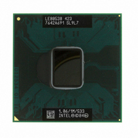
Manufacturer Part Number
LE80538VE0041M
Description
IC PROC CELERON M 1.06GHZ 479BGA
Manufacturer
Intel
Datasheet
1.LE80535NC013512.pdf
(69 pages)
Specifications of LE80538VE0041M
Processor Type
Celeron M
Features
533MHZ Bus, 1M L2 Cache
Speed
1.06GHz
Voltage
0.94V
Mounting Type
Surface Mount
Package / Case
479-BGA
Lead Free Status / RoHS Status
Lead free / RoHS Compliant
Other names
883549
Available stocks
Company
Part Number
Manufacturer
Quantity
Price


Intel
®
Table 25. Signal Description (Sheet 2 of 7)
Celeron
®
M Processor Datasheet
COMP[3:0]
D[63:0]#
DBR#
DBSY#
DEFER#
DINV[3:0]#
Name
Analog
Input/
Output
Output
Input/
Output
Input
Input/
Output
Type
COMP[3:0] must be terminated on the system board using precision (1%
tolerance) resistors. Refer to the platform design guides for more details on
implementation.
D[63:0]# (Data) are the data signals. These signals provide a 64-bit data path
between the FSB agents, and must connect the appropriate pins on both agents.
The data driver asserts DRDY# to indicate a valid data transfer.
D[63:0]# are quad-pumped signals and will thus be driven four times in a
common clock period. D[63:0]# are latched off the falling edge of both
DSTBP[3:0]# and DSTBN[3:0]#. Each group of 16 data signals correspond to a
pair of one DSTBP# and one DSTBN#. The following table shows the grouping
of data signals to data strobes and DINV# .
Quad-Pumped Signal Groups
Furthermore, the DINV# pins determine the polarity of the data signals. Each
group of 16 data signals corresponds to one DINV# signal. When the DINV#
signal is active, the corresponding data group is inverted and therefore sampled
active high.
DBR# (Data Bus Reset) is used only in processor systems where no debug port
is implemented on the system board. DBR# is used by a debug port interposer
so that an in-target probe can drive system reset. If a debug port is implemented
in the system, DBR# is a no connect. DBR# is not a processor signal.
DBSY# (Data Bus Busy) is asserted by the agent responsible for driving data on
the FSB to indicate that the data bus is in use. The data bus is released after
DBSY# is deasserted. This signal must connect the appropriate pins on both
FSB agents.
DEFER# is asserted by an agent to indicate that a transaction cannot be
guaranteed in-order completion. Assertion of DEFER# is normally the
responsibility of the addressed memory or Input/Output agent. This signal must
connect the appropriate pins of both FSB agents.
DINV[3:0]# (Data Bus Inversion) are source synchronous and indicate the
polarity of the D[63:0]# signals. The DINV[3:0]# signals are activated when the
data on the data bus is inverted. The bus agent will invert the data bus signals if
more than half the bits, within the covered group, would change level in the next
cycle.
DINV[3:0]# Assignment To Data Bus
D[15:0]#
D[31:16]#
D[47:32]#
D[63:48]#
DINV[3]#
DINV[2]#
DINV[1]#
DINV[0]#
Data Group
Bus Signal
0
1
2
3
DSTBN#/
DSTBP#
D[63:48]#
D[47:32]#
D[31:16]#
D[15:0]#
Data Bus Signals
Description
0
1
2
3
DINV#
57
Related parts for LE80538VE0041M
Image
Part Number
Description
Manufacturer
Datasheet
Request
R

Part Number:
Description:
Microprocessor: Intel Celeron M Processor 320 and Ultra Low Voltage Intel Celeron M Processor at 600MHz
Manufacturer:
Intel Corporation
Part Number:
Description:
Intel 82550 Fast Ethernet Multifunction PCI/CardBus Controller
Manufacturer:
Intel Corporation
Datasheet:
Part Number:
Description:
Intel StrataFlash memory 32 Mbit. Access speed 120 ns
Manufacturer:
Intel Corporation
Datasheet:
Part Number:
Description:
Intel StrataFlash memory 32 Mbit. Access speed 120 ns
Manufacturer:
Intel Corporation
Datasheet:
Part Number:
Description:
Intel StrataFlash memory 64 Mbit. Access speed 150 ns
Manufacturer:
Intel Corporation
Datasheet:
Part Number:
Description:
Intel StrataFlash memory 32 Mbit. Access speed 100 ns
Manufacturer:
Intel Corporation
Datasheet:
Part Number:
Description:
DA28F640J5A-1505 Volt Intel StrataFlash Memory
Manufacturer:
Intel Corporation
Datasheet:
Part Number:
Description:
5 Volt Intel StrataFlash?? Memory
Manufacturer:
Intel Corporation
Datasheet:
Part Number:
Description:
5 Volt Intel StrataFlash?? Memory
Manufacturer:
Intel Corporation
Part Number:
Description:
Intel 6300ESB I/O Controller Hub
Manufacturer:
Intel Corporation
Datasheet:
Part Number:
Description:
Intel 82801DB I/O Controller Hub (ICH4), Pb-Free SLI
Manufacturer:
Intel Corporation
Datasheet:
Part Number:
Description:
Intel 82801FB I/O Controller Hub (ICH6)
Manufacturer:
Intel Corporation
Datasheet:
Part Number:
Description:
Intel Strataflash Memory28F128J3 28F640J3 28F320J3
Manufacturer:
Intel Corporation
Datasheet:
Part Number:
Description:
Controllers, Intel 430TX PCIset: 82439TX System Controller (MTXC)
Manufacturer:
Intel Corporation