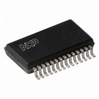
UDA1345TS/N2,118 NXP Semiconductors, UDA1345TS/N2,118 Datasheet - Page 20

UDA1345TS/N2,118
Manufacturer Part Number
UDA1345TS/N2,118
Description
IC AUDIO CODED 24BIT 28SSOP
Manufacturer
NXP Semiconductors
Type
Stereo Audior
Datasheet
1.UDA1345TSN2118.pdf
(29 pages)
Specifications of UDA1345TS/N2,118
Package / Case
28-SSOP (0.200", 5.30mm Width)
Data Interface
Serial
Resolution (bits)
24 b
Number Of Adcs / Dacs
2 / 2
Sigma Delta
Yes
S/n Ratio, Adcs / Dacs (db) Typ
94 / 98
Voltage - Supply, Analog
2.4 V ~ 3.6 V
Voltage - Supply, Digital
2.4 V ~ 3.6 V
Operating Temperature
-40°C ~ 85°C
Mounting Type
Surface Mount
Number Of Adc Inputs
2
Number Of Dac Outputs
2
Conversion Rate
100 KSPS
Interface Type
Serial (I2S) or L3
Resolution
24 bit
Maximum Operating Temperature
+ 85 C
Mounting Style
SMD/SMT
Minimum Operating Temperature
- 40 C
Number Of Channels
2 ADC/ 2 DAC
Lead Free Status / RoHS Status
Lead free / RoHS Compliant
Lead Free Status / RoHS Status
Lead free / RoHS Compliant, Lead free / RoHS Compliant
Other names
935266777118
UDA1345TSDB-T
UDA1345TSDB-T
UDA1345TSDB-T
UDA1345TSDB-T
Available stocks
Company
Part Number
Manufacturer
Quantity
Price
Part Number:
UDA1345TS/N2,118
Manufacturer:
NXP/恩智浦
Quantity:
20 000
NXP Semiconductors
11 AC CHARACTERISTICS (ANALOG)
V
(pins 1, 11, 22 and 27); unless otherwise specified.
Notes
1. The input voltage can be up to 2 V (RMS) when the current through the ADC input pin is limited to approximately
2. The input voltage to the ADC scales proportionally with the power supply voltage.
3. The output voltage of the DAC scales proportionally with the power supply voltage.
2002 May 28
Analog-to-digital converter
D
ΔV
(THD + N)/S total harmonic distortion-plus-noise
S/N
α
PSRR
Digital-to-analog converter
V
ΔV
(THD + N)/S total harmonic distortion plus
S/N
α
PSRR
DDD
cs
cs
SYMBOL
o(rms)
Economy audio CODEC
o
i
o
1 mA by using a series resistor.
= V
DDA
= V
digital output level at 1 V (RMS)
input voltage
unbalance between channels
to signal ratio
signal-to-noise ratio
channel separation
power supply rejection ratio
output voltage (RMS value)
unbalance between channels
noise-to-signal ratio
signal-to-noise ratio
channel separation
power supply rejection ratio
DDO
= 3.0 V; f
PARAMETER
i
= 1 kHz; f
s
= 44.1 kHz; T
notes 1 and 2
at 0 dB, 1 V (RMS)
at −60 dB, 1 mV (RMS);
A-weighted
V
f
V
note 3
at 0 dB
at −60 dB; A-weighted
code = 0; A-weighted
f
V
ripple
ripple
i
ripple(p-p)
ripple(p-p)
f
f
f
f
f
f
f
f
f
f
f
f
= 0 V; A-weighted
s
s
s
s
s
s
s
s
s
s
s
s
amb
= 44.1 kHz
= 96 kHz
= 44.1 kHz
= 96 kHz
= 44.1 kHz
= 96 kHz
= 44.1 kHz
= 96 kHz
= 44.1 kHz
= 96 kHz
= 44.1 kHz
= 96 kHz
= 1 kHz;
= 1 kHz;
20
CONDITIONS
= 25 °C; R
= 1%
= 1%
L
= 5 kΩ; all voltages referenced to ground
−2.5
−
−
−
−
−
90
90
−
−
850
−
−
−
−
−
90
90
−
−
MIN.
−1.5
0.1
−85
−80
−36
−34
96
94
100
30
900
0.1
−85
−80
−37
−35
100
98
100
60
TYP.
UDA1345TS
Product specification
950
−0.5
−
−80
−75
−30
−30
−
−
−
−
−
−80
−71
−30
−30
−
−
−
−
MAX.
dBFS
dB
dB
dB
dB
dB
dB
dB
dB
dB
mV
dB
dB
dB
dB
dB
dB
dB
dB
dB
UNIT


