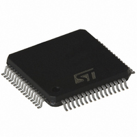
STLC5046 STMicroelectronics, STLC5046 Datasheet - Page 21

STLC5046
Manufacturer Part Number
STLC5046
Description
IC CODEC/FLTR PROG QUAD 64-TQFP
Manufacturer
STMicroelectronics
Type
PCM Codec/Filterr
Specifications of STLC5046
Data Interface
PCM Audio Interface
Resolution (bits)
16 b
Number Of Adcs / Dacs
4 / 4
Sigma Delta
Yes
Voltage - Supply, Analog
3.3 V ~ 5 V
Voltage - Supply, Digital
3.3 V ~ 5 V
Operating Temperature
-40°C ~ 85°C
Mounting Type
Surface Mount
Package / Case
64-TQFP, 64-VQFP
Lead Free Status / RoHS Status
Contains lead / RoHS non-compliant
Other names
497-3665
Available stocks
Company
Part Number
Manufacturer
Quantity
Price
Company:
Part Number:
STLC5046
Manufacturer:
ST
Quantity:
2 282
Part Number:
STLC5046
Manufacturer:
ST
Quantity:
20 000
Company:
Part Number:
STLC5046BCL
Manufacturer:
TOSHIBA
Quantity:
800
Company:
Part Number:
STLC5046BCP
Manufacturer:
ST
Quantity:
1 900
STLC5046
3.1.5
If bit 4 of CONF register (STA)=0
Dynamic I/O mode:
When CS1 is active D
outputs (see DIR register). For the I/O pins configured as inputs the corresponding D
be written by the values applied to those pins while CS1 is low.
If bit 4 of CONF register (STA)=1
Static I/O mode:
CIO0..3=0 The CS0..3 is a static input, DATA is written in DATA2 register bits 0..3.
CIO0..3=1 The CS0..3 is a static output, DATA is taken from DATA2 register bits 0..3.
Pin-strap value:
I/O Data register channel #2 (DATA2)
Addr=07h; Reset Value=00h
Addr=08h; Reset Value=X0h
If bit 4 of CONF register (STA)=0
Dynamic I/O mode:
When CS2 is active D2
outputs (see DIR register). For the I/O pins configured as inputs the corresponding D11..0
will be written by the values applied to those pins while CS2 is low.
Bit7
Bit7
Bit7
D1
D2
0
7
7
Bit6
D1
Bit6
Bit6
D2
0
6
6
11..0
11..0
are transferred to the corresponding I/O pins configured as
Bit5
Bit5
D1
Bit5
D2
are transferred to the corresponding I/O pins configured as
0
5
5
Doc ID 7052 Rev 5
Bit4
Bit4
Bit4
D1
D2
0
4
4
D1
CIO
D2
Bit3
D1
Bit3
Bit3
D2
0
0
11
11
3
3
3
D1
CIO
D2
Bit2
Bit2
Bit2
D1
D2
0
0
10
10
2
2
2
Registers addresses
CIO
Bit1
Bit1
Bit1
D1
D1
D2
D2
0
0
1
9
1
9
1
CIO
Bit0
Bit0
Bit0
11..0
D1
D1
D2
D2
0
0
21/51
0
8
0
8
0
will


