AT83C26-ZTUL Atmel, AT83C26-ZTUL Datasheet - Page 20
AT83C26-ZTUL
Manufacturer Part Number
AT83C26-ZTUL
Description
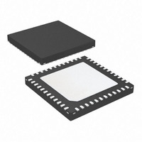
IC SMART CARD READER 1/PM 48-QFN
Manufacturer
Atmel
Datasheet
1.AT83C26-ALTUL.pdf
(77 pages)
Specifications of AT83C26-ZTUL
Controller Type
Smart Card Reader Interface
Interface
2-Wire
Voltage - Supply
3 V ~ 5.5 V
Current - Supply
65mA
Operating Temperature
-40°C ~ 85°C
Mounting Type
Surface Mount
Package / Case
48-VQFN Exposed Pad, 48-HVQFN, 48-SQFN, 48-DHVQFN
For Use With
AT89STK-09 - EVAL BOARD FOR AT83C26
Lead Free Status / RoHS Status
Lead free / RoHS Compliant


DC/DC converters
DC/DC A converter
Initialization Procedure for DC/DC A converter
20
AT83C26
The DC/DC A converter is controlled by VCARD1[1:0], SHUTDOWNA, ICCADJA, STEPREGA,
VCARD_OK1 and DEMBOOSTA[1:0] bits.
The DC/DC A converter cannot be switched on while the CPRES1 pin remains inactive. If
CPRES1 pin becomes inactive while the DC/DC A converter is operating an automatic shut
down sequence of the DC/DC A converter is initiated by the electronics.
A write operation in VCARD1[1:0] (0x01, 0x02, 0x03) starts the DC/DC. When the output voltage
remains within the voltage range specified by VCARD1[1:0], the VCARD_OK1 bit is set.
After a deactivation sequence (card extraction, DC/DC output voltage out of range, SHUT-
DOWNA bit =1...) the DC/DC A converter is automatically stopped.
It is mandatory to switch off the DC/DC A converter before entering in Power-down mode.
The DC/DC A Converter can work in two different modes which are selected by STEPREGA bit:
•
•
The current drawn from power supply by the DC/DC A converter is controlled during the startup
phase in order to avoid high transient current mainly in Pump Mode which could cause the
power supply voltage to drop dramatically. This control is done by means of bits DEM-
BOOSTA[1:0], which increases progressively the startup current level.
The DC/DCA sensitivity to any overflow current can be modified (20%) by using the ICCADJA bit
(SC1_CFG3 register).
The initialization procedure is described in flow chart:
•
•
•
While VCC1 remains higher than 3.6V and startup current lower than 30 mA (depending on the
load type), the DC/DC A converter should be ready without having to increment DEM-
BOOSTA[1:0] bits beyond [0:0] level. If at least one of the two conditions are not met (VCC <
3.6V or startup current > 30 mA), it will be necessary to increment the DEMBOOSTA[1:0] bits
until the DC/DC converter is ready.
Increment of DEMBOOSTA[1:0] bits increases at the same time the current overflow level in the
same proportion as the startup current. So once the DC/DC converter is ready it advised to dec-
rement the DEMBOOSTA[1:0] bits to restore the overflow current to its normal or desired value.
Pump Mode (STEPREGA = 0): an external inductance of 10 µH must be connected
between pins LIA and VCC. VCC can be higher or lower than CVCC1.
Regulator mode (STEPREGA = 1): no external inductance is required but VCC must be
always higher than CVCC+0.3V.
Select the CVCC1 level by means of bits VCARD1[1:0] in SC1_CFG0 register,
Set bits DEMBOOSTA[1:0] in SC1_CFG4 register following the current level control wanted.
Monitor VCARD_OK1 bit in SC1_STATUS register in order to know when the DC/DC A
Converter is ready (CVCC1 voltage has reached the expected level)
7511D–SCR–02/07
Related parts for AT83C26-ZTUL
Image
Part Number
Description
Manufacturer
Datasheet
Request
R

Part Number:
Description:
SMART CARD READER INTERFACE WITH POWER MANAGEMENT
Manufacturer:
ATMEL [ATMEL Corporation]
Datasheet:

Part Number:
Description:
IC SMART CARD READER 1/PM 48VQFP
Manufacturer:
Atmel
Datasheet:
Part Number:
Description:
IC SMART CARD READER 1/PM 48VQFP
Manufacturer:
Atmel
Datasheet:
Part Number:
Description:
IC SMART CARD READER 3/5V 48VQFP
Manufacturer:
Atmel
Datasheet:

Part Number:
Description:
IC SMART CARD READER 1/PM 48-MLF
Manufacturer:
Atmel
Datasheet:

Part Number:
Description:
RFID Modules & Development Tools 3V Smart card reader
Manufacturer:
Atmel
Datasheet:

Part Number:
Description:
Multiple Smart Card Reader Interface With Power Management
Manufacturer:
ATMEL Corporation
Datasheet:

Part Number:
Description:
DEV KIT FOR AVR/AVR32
Manufacturer:
Atmel
Datasheet:
Part Number:
Description:
INTERVAL AND WIPE/WASH WIPER CONTROL IC WITH DELAY
Manufacturer:
ATMEL Corporation
Datasheet:
Part Number:
Description:
Low-Voltage Voice-Switched IC for Hands-Free Operation
Manufacturer:
ATMEL Corporation
Datasheet:
Part Number:
Description:
MONOLITHIC INTEGRATED FEATUREPHONE CIRCUIT
Manufacturer:
ATMEL Corporation
Datasheet:
Part Number:
Description:
AM-FM Receiver IC U4255BM-M
Manufacturer:
ATMEL Corporation
Datasheet:
Part Number:
Description:
Monolithic Integrated Feature Phone Circuit
Manufacturer:
ATMEL Corporation
Datasheet:
Part Number:
Description:
Multistandard Video-IF and Quasi Parallel Sound Processing
Manufacturer:
ATMEL Corporation
Datasheet: