DS21Q42T Maxim Integrated Products, DS21Q42T Datasheet - Page 59

DS21Q42T
Manufacturer Part Number
DS21Q42T
Description
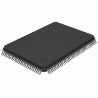
IC FRAMER ENHANCED T1 4X 128TQFP
Manufacturer
Maxim Integrated Products
Datasheet
1.DS21Q42T.pdf
(116 pages)
Specifications of DS21Q42T
Controller Type
T1 Framer
Interface
Parallel/Serial
Voltage - Supply
2.97 V ~ 3.63 V
Current - Supply
75mA
Operating Temperature
0°C ~ 70°C
Mounting Type
Surface Mount
Package / Case
128-TQFP, 128-VQFP
Lead Free Status / RoHS Status
Contains lead / RoHS non-compliant
Available stocks
Company
Part Number
Manufacturer
Quantity
Price
Part Number:
DS21Q42T
Manufacturer:
DALLAS
Quantity:
20 000
13.3 Minimum Delay Synchronous RSYSCLK/TSYSCLK Mode
In applications where the framer is connected to backplanes that are frequency locked to the recovered T1
clock (i.e., the RCLK output), the full two frame depth of the onboard elastic stores is really not needed.
In fact, in some delay sensitive applications, the normal two frame depth may be excessive. Register bits
CCR3.7 and CCR3.0 control the RX and TX elastic stores depths. In this mode, RSYSCLK and
TSYSCLK must be tied together and they must be frequency locked to RCLK. All of the slip contention
logic in the framer is disabled (since slips cannot occur). Also, since the buffer depth is no longer two
frames deep, the framer must be set up to source a frame pulse at the RSYNC pin and this output must be
tied to the TSSYNC input. On power–up after the RSYSCLK and TSYSCLK signals have locked to the
RCLK signal, the elastic stores should be reset.
14.
The DS21Q42 has an enhanced HDLC controller configurable for use with the Facilities Data Link or
DS0s. There are 64 byte buffers in both the transmit and receive paths. The user can select any DS0 or
multiple DS0s as well as any specific bits within the DS0(s) to pass through the HDLC controller. See
Figure 20-15 for details on formatting the transmit side. Note that TBOC.6 = 1 and TDC1.7 = 1 cannot
exist without corrupting the data in the FDL. For use with the FDL, see section 15.1. See Table 14-1 for
configuring the transmit HDLC controller.
Four new registers were added for the enhanced functionality of the HDLC controller; RDC1, RDC2,
TDC1, and TDC2. Note that the BOC controller is functional when the HDLC controller is used for
DS0s. Section 15 contains all of the HDLC and BOC registers and information on FDL/Fs Extraction
and Insertion with and without the HDLC controller.
Table 14-1. TRANSMIT HDLC CONFIGURATION
DS0(s)
FDL
Disable
14.1 HDLC for DS0s
When using the HDLC controllers for DS0s, the same registers shown in section 15 will be used except
for the TBOC and RBOC registers and bits HCR.7, HSR.7, and HIMR.7. As a basic guideline for
interpreting and sending HDLC messages and BOC messages, the following sequences can be applied.
Receive a HDLC Message
1) Enable RPS interrupts.
2) Wait for interrupt to occur.
3) Disable RPS interrupt and enable either RPE, RNE, or RHALF interrupt.
4) Read RHIR to obtain REMPTY status.
5) Repeat Step 4.
6) Wait for interrupt, skip to Step 4.
7) If POK = 0, then discard whole packet; if POK = 1, accept the packet.
8) Disable RPE, RNE, or RHALF interrupt, enable RPS interrupt and return to Step 1.
FUNCTION
HDLC CONTROLLER
a) If REMPTY = 0, then record OBYTE, CBYTE, and POK bits and then read the FIFO.
b) If REMPTY=1, then skip to Step 6.
a1) If CBYTE = 0, then skip to Step 5.
a2) If CBYTE = 1, then skip to Step 7.
TBOC.6
0
1
0
TDC1.7
1
0
0
59 of 116
TCR1.2
1 or 0
1 or 0
1


