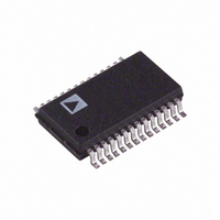
AD9850BRSZ Analog Devices Inc, AD9850BRSZ Datasheet - Page 8

AD9850BRSZ
Manufacturer Part Number
AD9850BRSZ
Description
IC DDS SYNTHESIZER CMOS 28-SSOP
Manufacturer
Analog Devices Inc
Datasheet
1.AD9850BRSZ-REEL.pdf
(20 pages)
Specifications of AD9850BRSZ
Mounting Type
Surface Mount
Resolution (bits)
10 b
Master Fclk
125MHz
Tuning Word Width (bits)
32 b
Voltage - Supply
3.3V, 5V
Operating Temperature
-40°C ~ 85°C
Package / Case
28-SSOP
Rf Ic Case Style
SSOP
No. Of Pins
28
Supply Voltage Range
4.75V To 5.25V, 3.3V
Operating Temperature Range
-40°C To +85°C
Msl
MSL 3 - 168 Hours
Frequency Max
125MHz
Current Rating
30A
Frequency
125MHz
Rohs Compliant
Yes
Lead Free Status / RoHS Status
Lead free / RoHS Compliant
AD9850
THEORY OF OPERATION AND APPLICATION
The AD9850 uses direct digital synthesis (DDS) technology, in the
form of a numerically controlled oscillator, to generate a frequency/
phase-agile sine wave. The digital sine wave is converted to analog
form via an internal 10-bit high speed D/A converter, and an
on-board high speed comparator is provided to translate the analog
sine wave into a low jitter TTL/CMOS compatible output square
wave. DDS technology is an innovative circuit architecture that
allows fast and precise manipulation of its output frequency under
full digital control. DDS also enables very high resolution in the
incremental selection of output frequency; the AD9850 allows an
output frequency resolution of 0.0291 Hz with a 125 MHz refer-
ence clock applied. The AD9850’s output waveform is phase con-
tinuous when changed.
The basic functional block diagram and signal flow of the
AD9850 configured as a clock generator is shown in Figure 4.
The DDS circuitry is basically a digital frequency divider function
whose incremental resolution is determined by the frequency of
the reference clock divided by the 2
tuning word. The phase accumulator is a variable-modulus
counter that increments the number stored in it each time it
receives a clock pulse. When the counter overflows, it wraps
around, making the phase accumulator’s output contiguous.
IF IN
PROCESSOR
Rx
Figure 1. Basic AD9850 Clock Generator Application
with Low-Pass Filter
Figure 2. AD9850 Clock Generator Application in a
Spread-Spectrum Receiver
VCA
XTAL
OSC
LOCKED TO Tx CHIP/
REFERENCE
SYMBOL PN RATE
125MHz
CLOCK
DATA
LOW-PASS
BUS
I/Q MIXER
FILTER
AND
FREQUENCY
ADC CLOCK
8-b
OR 1-b
RESET, AND 2
CLOCK LINES
CLK
Q
5 PARALLEL DATA,
I
+V
AD9850
GENERATOR
DUAL 8-BIT
S
AD9059
40 SERIAL DATA,
AD9850
CLOCK
ADC
RSET
ADC ENCODE
GND
QOUTB
IOUTB
QOUT
8
8
IOUT
VINN
VINP
CHIP/SYMBOL/PN
32
N
RATE DATA
DEMODULATOR
number of bits in the
100k
100k
DIGITAL
COMP
OUTPUTS
CLOCK
CMOS
5-POLE ELLIPTICAL
42MHz LOW-PASS
200
200
100
470pF
AGC
LOW-PASS
FILTER
IMPEDANCE
Rx
BASEBAND
DIGITAL
DATA
OUT
TRUE
200
–8–
The frequency tuning word sets the modulus of the counter,
which effectively determines the size of the increment (∆ Phase)
that is added to the value in the phase accumulator on the next
clock pulse. The larger the added increment, the faster the
accumulator overflows, which results in a higher output fre-
quency. The AD9850 uses an innovative and proprietary
algorithm that mathematically converts the 14-bit truncated
value of the phase accumulator to the appropriate COS value.
This unique algorithm uses a much reduced ROM look-up table
and DSP techniques to perform this function, which contributes
to the small size and low power dissipation of the AD9850. The
relationship of the output frequency, reference clock, and tuning
word of the AD9850 is determined by the formula
where:
∆ Phase is the value of the 32-bit tuning word.
CLKIN is the input reference clock frequency in MHz.
f
The digital sine wave output of the DDS block drives the inter-
nal high speed 10-bit D/A converter that reconstructs the sine
wave in analog form. This DAC has been optimized for dynamic
performance and low glitch energy as manifested in the low
jitter performance of the AD9850. Because the output of the
REFERENCE
OUT
3c. Digitally-Programmable Divide-by-N Function in PLL
125MHz
CLOCK
is the frequency of the output signal in MHz.
Figure 3. AD9850 Complete DDS Synthesizer in
Frequency Up-Conversion Applications
3b. Frequency/Phase–Agile Reference for PLL
FREQUENCY
3a. Frequency/Phase–Agile Local Oscillator
FREQUENCY
REF
REFERENCE
COMPLETE
FILTER
AD9850
TUNING
125MHz
WORD
DDS
IN
IF
f
OUT
COMPARATOR
TUNING WORD
COMPLETE
AD9850
= (∆ Phase × CLKIN)/2
PHASE
FILTER
DDS
COMPLETE DDS
AD9850
FILTER
COMPARATOR
DIVIDE-BY-N
PROGRAMMABLE
PHASE
DIVIDE-BY-N
FILTER
LOOP
FUNCTION
FILTER
TUNING
WORD
VCO
FILTER
LOOP
RF
FREQUENCY
OUT
32
FREQUENCY
OUT
RF
VCO
FREQUENCY
OUT
REV. H
RF


