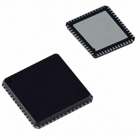
AD9911BCPZ Analog Devices Inc, AD9911BCPZ Datasheet - Page 20

AD9911BCPZ
Manufacturer Part Number
AD9911BCPZ
Description
IC DDS 500MSPS DAC 10BIT 56LFCSP
Manufacturer
Analog Devices Inc
Datasheet
1.AD9911BCPZ-REEL7.pdf
(44 pages)
Specifications of AD9911BCPZ
Resolution (bits)
10 b
Master Fclk
500MHz
Tuning Word Width (bits)
32 b
Voltage - Supply
1.71 V ~ 1.96 V
Operating Temperature
-40°C ~ 85°C
Mounting Type
Surface Mount
Package / Case
56-LFCSP
Transmitting Current
73mA
Data Rate
800Mbps
Rf Ic Case Style
LFCSP
No. Of Pins
56
Supply Voltage Range
1.71V To 1.89V, 3.135V To 3.465V
Operating Temperature Range
-40°C To +85°C
Msl
MSL 3 - 168 Hours
Lead Free Status / RoHS Status
Lead free / RoHS Compliant
For Use With
AD9911/PCBZ - BOARD EVAL FOR AD9911AD9911/PCB - BOARD EVAL FOR AD9911
Lead Free Status / Rohs Status
Compliant
Available stocks
Company
Part Number
Manufacturer
Quantity
Price
Company:
Part Number:
AD9911BCPZ
Manufacturer:
NXP
Quantity:
173
Part Number:
AD9911BCPZ
Manufacturer:
ADI/亚德诺
Quantity:
20 000
AD9911
TEST-TONE MODE
Test-tone mode enables sinusoidal amplitude modulation of the
carrier (CH1). Setting Bit 2 in Register 0x01 enables test-tone
mode. Auxiliary CH2 and CH3 should both be disabled using
the channel enable bits (CSR Bit <7>). The frequency of
modulation is set using the frequency tuning word
(Register 0x04 Bits <31:0>) of auxiliary CH0. Auxiliary CH0
output scalar (Register 0x06 Bits <0:9>) sets the magnitude of
the modulating signal. See Figure 37 for a diagram of the test-
tone mode configuration.
REFERENCE CLOCK MODES
The AD9911 supports several methods for generating the
internal system clock. An on-chip oscillator circuit is available
for initiating the low frequency reference signal by connecting
a crystal to the clock input pins. The system clock can also be
generated using the internal, PLL-based reference clock
multiplier, allowing the part to operate with a low frequency
clock source while still providing a high sample rate for the
DDS and DAC. For best phase noise performance, a clean,
stable clock with a high slew rate is required.
PHASE OFFSET
Figure 37. Test-Tone Mode Configuration
14
DDS CORE 1
DDS CORE 0
COS(X)
COS(X)
10
AMPLITUDE
10
10
DDS CORE 1
DDS CORE 0
DDS CORE 2
DDS CORE 3
10
Figure 36. SpurKiller/Multitone Mode Configuration
DAC 1
COS(X)
COS(X)
COS(X)
COS(X)
Rev. 0 | Page 20 of 44
10
10
10
10
CFR <18:16>
CFR <18:16>
CFR <18:16>
ALIGN
ALIGN
ALIGN
DATA
DATA
DATA
Enabling the PLL allows multiplication of the reference clock
frequency from 4× to 20×, in integer steps. The PLL multiplica-
tion value is 5-bits located in the Function Register 1 (FR1) Bits
<22:18>. For further information, refer to the Register Map
section.
When FR1 <22:18> is programmed with values ranging from 4 to
20 (decimal), the clock multiplier is enabled. The integer value in
the register represents the multiplication factor. The system clock
rate with the clock multiplier enabled is equal to the reference clock
rate times the multiplication factor. If FR1 <22:18> is programmed
with a value less than 4 or greater than 20, the clock multiplier is
disabled. Note that the output frequency of the PLL has a restricted
frequency range. There is a VCO gain bit that must be set
appropriately. The VCO gain bit (FR1<23>) defines two ranges
(low/high) of frequency output. See the Register Map section for
configuration directions and defaults.
The charge pump current in the PLL defaults to 75
typically produces the best phase noise characteristics.
Increasing charge pump current typically degrades phase noise,
but decreases the lock time and alters the loop bandwidth. The
charge pump control bits (FR1 <17:16>) function is described
in the Register Map section.
To enable the on-chip oscillator for crystal operation, drive
CLK_MODE_SEL (Pin 24) high. The CLKMODESEL pin is
considered an analog input, operating on 1.8 V logic. With the
on-chip oscillator enabled, connection of an external crystal to
the REF_CLK and REF_CLKB inputs is made producing a low
frequency reference clock. The crystal frequency must be in the
range of 20 MHz to 30 MHz. summarizes the clock mode
options. See the Register Maps section for more details.
3
3
3
10
10
10
10
MUX
10
10-BIT DAC
0
DAC 1
μA,
which


