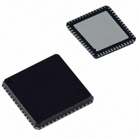
AD9911BCPZ Analog Devices Inc, AD9911BCPZ Datasheet - Page 35

AD9911BCPZ
Manufacturer Part Number
AD9911BCPZ
Description
IC DDS 500MSPS DAC 10BIT 56LFCSP
Manufacturer
Analog Devices Inc
Datasheet
1.AD9911BCPZ-REEL7.pdf
(44 pages)
Specifications of AD9911BCPZ
Resolution (bits)
10 b
Master Fclk
500MHz
Tuning Word Width (bits)
32 b
Voltage - Supply
1.71 V ~ 1.96 V
Operating Temperature
-40°C ~ 85°C
Mounting Type
Surface Mount
Package / Case
56-LFCSP
Transmitting Current
73mA
Data Rate
800Mbps
Rf Ic Case Style
LFCSP
No. Of Pins
56
Supply Voltage Range
1.71V To 1.89V, 3.135V To 3.465V
Operating Temperature Range
-40°C To +85°C
Msl
MSL 3 - 168 Hours
Lead Free Status / RoHS Status
Lead free / RoHS Compliant
For Use With
AD9911/PCBZ - BOARD EVAL FOR AD9911AD9911/PCB - BOARD EVAL FOR AD9911
Lead Free Status / Rohs Status
Compliant
Available stocks
Company
Part Number
Manufacturer
Quantity
Price
Company:
Part Number:
AD9911BCPZ
Manufacturer:
NXP
Quantity:
173
Part Number:
AD9911BCPZ
Manufacturer:
ADI/亚德诺
Quantity:
20 000
REGISTER MAPS
CONTROL REGISTER MAP
Table 24.
Register
Name
(Address)
Channel
Select
Register
(CSR)
(0x00)
Function
Register 1
(FR1)
(0x01)
Function
Register 2
(FR2)
(0x02)
1
Channel enable bits do not require an I/O update to be activated. These bits are active immediately after the byte containing the bits is written. All other bits need an
I/O update to become active. The channel enable bits determine if the channel registers and/or profile registers are written to or not.
Bit
Range
<7:0>
<7:0>
<15:8>
<23:16>
<7:0>
<15:8>
Bit 7 (MSB)
Auxiliary
Channel 3
(W/R enable
Reference clock
input power
down
Open
VCO gain control
Multidevice
synchronization
slave enable
All channels auto
clear sweep
accumulator
1
)
Bit 6
Auxiliary
Channel 2
(W/R enable
External power
down mode
Multidevice
synchronization
master enable
All channels
clear sweep
accumulator
1
)
Profile pin configuration <14:12>
Bit 5
Primary Channel 1
(W/R enable
Sync clock
disable
Multidevice
synchronization
status
All channels auto
clear phase
accumulator
PLL divider ratio <22:18>
Rev. 0 | Page 35 of 44
1
)
Bit 4
Auxiliary
Channel 0
(W/R enable
DAC reference
power down
Multidevice
synchronization
mask
All channels
clear phase
accumulator
1
)
Bit 3
Must
be 0
Open
Open <3:2>
Open <11:10>
Ramp up/ramp
down <11:10>
Bit 2
I/0 mode select <2:1>
Test-
tone
enable
System clock offset <1:0>
Bit 1
Manual
hardware
synchronization
Charge pump control <17:16>
Open <9:8>
Modulation Level <9:8>
Bit 0 (LSB)
Manual software
synchronization
LSB first
AD9911
Default
Value
0xF0
0x00
0x00
0x00
0x00
0x00


