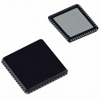
AD9911BCPZ Analog Devices Inc, AD9911BCPZ Datasheet - Page 4

AD9911BCPZ
Manufacturer Part Number
AD9911BCPZ
Description
IC DDS 500MSPS DAC 10BIT 56LFCSP
Manufacturer
Analog Devices Inc
Datasheet
1.AD9911BCPZ-REEL7.pdf
(44 pages)
Specifications of AD9911BCPZ
Resolution (bits)
10 b
Master Fclk
500MHz
Tuning Word Width (bits)
32 b
Voltage - Supply
1.71 V ~ 1.96 V
Operating Temperature
-40°C ~ 85°C
Mounting Type
Surface Mount
Package / Case
56-LFCSP
Transmitting Current
73mA
Data Rate
800Mbps
Rf Ic Case Style
LFCSP
No. Of Pins
56
Supply Voltage Range
1.71V To 1.89V, 3.135V To 3.465V
Operating Temperature Range
-40°C To +85°C
Msl
MSL 3 - 168 Hours
Lead Free Status / RoHS Status
Lead free / RoHS Compliant
For Use With
AD9911/PCBZ - BOARD EVAL FOR AD9911AD9911/PCB - BOARD EVAL FOR AD9911
Lead Free Status / Rohs Status
Compliant
Available stocks
Company
Part Number
Manufacturer
Quantity
Price
Company:
Part Number:
AD9911BCPZ
Manufacturer:
NXP
Quantity:
173
Part Number:
AD9911BCPZ
Manufacturer:
ADI/亚德诺
Quantity:
20 000
AD9911
SPECIFICATIONS
AVDD and DVDD = 1.8 V ± 5%; DVDD_I/O = 3.3 V ± 5%; R
multiplier bypassed), unless otherwise noted.
Table 1.
Parameter
REF CLOCK INPUT CHARACTERISTICS
DAC OUTPUT CHARACTERISTICS
WIDEBAND SFDR
WIDEBAND SFDR Improvement
Full-Scale Output Current
Gain Error
Output Current Offset
Differential Nonlinearity
Integral Nonlinearity
Output Capacitance
Voltage Compliance Range
1 MHz to 20 MHz Analog Output
20 MHz to 60 MHz Analog Output
60 MHz to 100 MHz Analog Output
100 MHz to 150 MHz Analog Output
150 t MHz to 200 MHz Analog Output
60 MHz to 100 MHz Analog Output
100 MHz to 150 MHz Analog Output
150 MHz to 200 MHz Analog Output
Frequency Range
Input Power Sensitivity
Input Voltage Bias Level
Input Capacitance
Input Impedance
Duty Cycle with REF_CLK Multiplier Bypassed
Duty Cycle with REF_CLK Multiplier Enabled
CLK Mode Select (Pin 24) Logic 1 V
CLK Mode Select (Pin 24) Logic 0 V
Spur Reduction Enabled
REF_CLK Multiplier Enabled
Internal VCO Output Frequency Range
Internal VCO Output Frequency Range
Crystal REF_CLK Source Range
REF_CLK Multiplier Bypassed
VCO Gain Bit Set
VCO Gain Bit Cleared
1
Min
1
10
255
100
20
−5
45
35
1.25
−10
AVDD –
0.50
Rev. 0 | Page 4 of 44
10
Typ
1.15
2
1500
1
±0.5
±1.0
3
−65
−62
−59
−56
−53
8
15
12
SET
= 1.91 kΩ; external reference clock frequency = 500 MSPS (REF_CLK
Max
500
125
500
160
30
+3
55
65
1.8
0.5
+10
25
AVDD +
0.50
Unit
mA
MHz
MHz
MHz
MHz
MHz
dBm
V
pF
Ω
%
%
V
V
%FS
μA
LSB
LSB
pF
V
dBc
dBc
dBc
dBc
dBc
dBc
dBc
dBc
Test Conditions/Comments
Measured at the pin (single-ended)
1.8 V digital input logic
1.8 V digital input logic
Must be referenced to AVDD
10 mA is set by R
The frequency range for wideband SFDR is
defined as dc to Nyquist
Programs devices on an individual basis to
enable spur reduction. See the
SpurKiller/Multitone Mode section.
SET
= 1.91 kΩ


