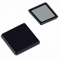
AD9911BCPZ Analog Devices Inc, AD9911BCPZ Datasheet - Page 40

AD9911BCPZ
Manufacturer Part Number
AD9911BCPZ
Description
IC DDS 500MSPS DAC 10BIT 56LFCSP
Manufacturer
Analog Devices Inc
Datasheet
1.AD9911BCPZ-REEL7.pdf
(44 pages)
Specifications of AD9911BCPZ
Resolution (bits)
10 b
Master Fclk
500MHz
Tuning Word Width (bits)
32 b
Voltage - Supply
1.71 V ~ 1.96 V
Operating Temperature
-40°C ~ 85°C
Mounting Type
Surface Mount
Package / Case
56-LFCSP
Transmitting Current
73mA
Data Rate
800Mbps
Rf Ic Case Style
LFCSP
No. Of Pins
56
Supply Voltage Range
1.71V To 1.89V, 3.135V To 3.465V
Operating Temperature Range
-40°C To +85°C
Msl
MSL 3 - 168 Hours
Lead Free Status / RoHS Status
Lead free / RoHS Compliant
For Use With
AD9911/PCBZ - BOARD EVAL FOR AD9911AD9911/PCB - BOARD EVAL FOR AD9911
Lead Free Status / Rohs Status
Compliant
Available stocks
Company
Part Number
Manufacturer
Quantity
Price
Company:
Part Number:
AD9911BCPZ
Manufacturer:
NXP
Quantity:
173
Part Number:
AD9911BCPZ
Manufacturer:
ADI/亚德诺
Quantity:
20 000
AD9911
CFR <6> = 0 (default). The DAC is enabled for operation.
CFR <6> = 1. The DAC is disabled and held in its lowest power
dissipation state.
CFR <7> digital power-down.
CFR <7> = 0 (default). The digital core is enabled for operation.
CFR <7> = 1. The digital core is disabled and is in its lowest
power dissipation state.
CFR <9:8>. DAC LSB control (see Table 5).
CFR <9:8> = 00 (default).
CFR <10> must be cleared to 0.
CFR <13> linear sweep ramp rate load at I/O_UPDATE.
CFR <13> = 0 (default). The linear sweep ramp rate timer is
loaded only upon timeout (timer = 1); it is not loaded by the
I/O_UPDATE input signal.
CFR <13> = 1. The linear sweep ramp rate timer is loaded upon
timeout (timer = 1) or at the time of an I/O_UPDATE input
signal.
CFR <14> linear sweep enable.
CFR <14> = 0 (default). The linear sweep capability of the
AD9911 is inactive. CFR <14> = 1. The linear sweep capability
of the AD9911 is active. The delta frequency tuning word is
applied to the frequency accumulator at the programmed
ramp rate.
CFR <15> linear sweep no-dwell.
CFR <15> = 0 (default). The linear sweep no-dwell function is
inactive. CFR <15> = 1. The linear sweep no-dwell function is
active. See the Linear Sweep (Shaped) Modulation Mode
section for details. If CFR <14> is clear, this bit is ignored.
CFR <18:16> Data align bits for SpurKiller mode. See the
SpurKiller/Multitone Mode section for details.
CFR <21:19> inactive.
CFR <23:22> amplitude/frequency/phase select controls, the
type of modulation is to be performed for that channel. See the
Shift Keying Mode section for examples.
Channel Frequency Tuning Word 0 (CFTW0) Description
CFTW0 <32:0> Frequency Tuning Word 0 for each channel.
Rev. 0 | Page 40 of 44
Channel Phase Offset Word 0 (CPOW0) Description
CPOW0 <13:0> Phase Offset Word 0 for each channel.
CPOW0 <15:14> inactive.
Amplitude Control Register (ACR) Description
ACR <9:0> amplitude scale factor.
ACR <10> amplitude ramp rate load control bit.
ACR <10> = 0 (default). The amplitude ramp rate timer is
loaded only upon timeout (timer = 1) and is not loaded by an
I/O_UPDATE input signal (or change in the profile select bits).
ACR <10> = 1. The amplitude ramp rate timer is loaded upon
timeout (timer =1) or at the time of an I/O_UPDATE input
signal (or change in profile select bits).
ACR <11> auto RU/RD enable (only valid when ACR <12> is
active high).
ACR <11> = 0 (default). When ACR <12> is active, Logic 0 on
ACR <11> enables the manual RU/RD operation. See the
Output Amplitude Control section of this document for details.
ACR <11> = 1. If ACR <12> is active, a Logic 1 on ACR <11>
enables the AUTO RU/RD operation. See the Output
Amplitude Control section for details.
ACR <12> amplitude multiplier enable.
ACR <12> = 0 (default). Amplitude multiplier is disabled. The
associated clocks are stopped for power saving; the data from
the DDS core is routed around the multipliers.
ACR <12> = 1, amplitude multiplier is enabled.
ACR <13> inactive.
ACR <15:14> amplitude increment/decrement step size. See
Table 20 for details.
ACR <23:16> amplitude ramp rate value.
Channel Linear Sweep Register (LSR) Description
LSR <15:0> linear sweep rising ramp rate.
Channel Linear Sweep Rising Delta Word Register (RDW)
Description
RDW <31:0> 32-bit rising delta tuning word.
Channel Linear Sweep Falling Delta Word Register
(FDW) Description
FDW <31:0> 32-bit falling delta tuning word.


