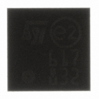
STSMIA832TBR STMicroelectronics, STSMIA832TBR Datasheet - Page 11

STSMIA832TBR
Manufacturer Part Number
STSMIA832TBR
Description
IC LINE RCVR 1.8V/2.8V 25-TFBGA
Manufacturer
STMicroelectronics
Type
Receiverr
Datasheet
1.STSMIA832TBR.pdf
(25 pages)
Specifications of STSMIA832TBR
Number Of Drivers/receivers
0/1
Protocol
SMIA
Voltage - Supply
2.65 V ~ 3.6 V
Mounting Type
Surface Mount
Package / Case
25-µTFBGA
Lead Free Status / RoHS Status
Lead free / RoHS Compliant
Other names
497-5147-2
Available stocks
Company
Part Number
Manufacturer
Quantity
Price
Company:
Part Number:
STSMIA832TBR
Manufacturer:
st
Quantity:
23
Company:
Part Number:
STSMIA832TBR
Manufacturer:
STMicroelectronics
Quantity:
10 000
Part Number:
STSMIA832TBR
Manufacturer:
ST
Quantity:
20 000
STSMIA832
Figure 9.
3.7
3.8
STSMIA832 load capacitance and rise and fall time of LVTTL parallel outputs
Board layout
To obtain the maximum benefit from the noise and EMI reductions of subLVDS, attention
should be paid to the layout of differential lines. Lines of a differential pair should always be
adjacent to eliminate noise interference from other signals and take full advantage of the
noise canceling of the differential signals. Equal length should be maintained on signal
traces for a given differential pair. As with any high-speed design, the impedance
discontinuities should be limited (reduce the numbers of vias and no 90 degree angles on
traces). Any discontinuities which do occur on one signal line should be mirrored in the other
line of the differential pair. Care should be taken to ensure that the differential trace
impedance match the differential impedance of the selected physical media (this impedance
should also match the value of the termination resistor (100 ohm) that is connected across
the differential pair at the receiver’s input). Surface mount resistors are recommended to
avoid the additional inductance that accompanies leaded resistors.
These resistors should be placed as close as possible to the receiver input pins to reduce
stubs and effectively terminate the differential lines. All of these considerations will limit
reflections and crosstalk which adversely effect high frequency performance and EMI.
Decoupling capacitors
Bypassing capacitors are needed to reduce the impact of switching noise which could limit
performance. For a conservative approach three parallel-connected decoupling capacitors
(multi-layered ceramic capacitors in surface mount form factor) between each V
ground plane(s) are recommended. An example is shown in the figure below. Wide traces
for power and ground should be used and it should be ensured each capacitor has its own
via to the ground plane.
Doc ID 12174 Rev 5
Application information
CC
and the
11/25


