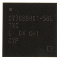
CY7C68001-56LTXC Cypress Semiconductor Corp, CY7C68001-56LTXC Datasheet - Page 24

CY7C68001-56LTXC
Manufacturer Part Number
CY7C68001-56LTXC
Description
IC USB EZ-USB SX2 HS 56VQFN
Manufacturer
Cypress Semiconductor Corp
Series
CY7Cr
Type
USBr
Specifications of CY7C68001-56LTXC
Protocol
USB 2.0
Voltage - Supply
3 V ~ 3.6 V
Mounting Type
Surface Mount
Package / Case
56-VQFN Exposed Pad, 56-HVQFN, 56-SQFN, 56-DHVQFN
Lead Free Status / RoHS Status
Lead free / RoHS Compliant
Number Of Drivers/receivers
-
Lead Free Status / Rohs Status
Lead free / RoHS Compliant
Other names
428-2932
Available stocks
Company
Part Number
Manufacturer
Quantity
Price
Part Number:
CY7C68001-56LTXC
Manufacturer:
CYPRESS/赛普拉斯
Quantity:
20 000
7.3.3
This flag selects the polarity of the SLOE pin. If SLOE = 0 (default), the polarity is active LOW. If SLOE = 1, the polarity is active
HIGH. This bit can only be changed by using the EEPROM configuration load.
7.3.4
This flag selects the polarity of the SLRD pin. If SLRD = 0 (default), the polarity is active LOW. If SLRD = 1, the polarity is active
HIGH. This bit can only be changed by using the EEPROM configuration load.
7.3.5
This flag selects the polarity of the SLWR pin. If SLWR = 0 (default), the polarity is active LOW. If SLWR = 1, the polarity is active
HIGH. This bit can only be changed by using the EEPROM configuration load.
7.3.6
This flag selects the polarity of the EF pin (FLAGA/B/C/D). If EF = 0 (default), the EF pin is pulled low when the FIFO is empty.
If EF = 1, the EF pin is pulled HIGH when the FIFO is empty.
7.3.7
This flag selects the polarity of the FF pin (FLAGA/B/C/D). If FF = 0 (default), the FF pin is pulled low when the FIFO is full. If
FF = 1, the FF pin is pulled HIGH when the FIFO is full.
7.4
These register bits define the silicon revision.
The upper nibble is the major revision. The lower nibble is the minor revision. For example: if REVID = 0x11, then the silicon
revision is 1.1.
7.5
These registers configure the large, data-handling SX2 endpoints, EP2, 4, 6, and 8. Figure 3-1 shows the configuration choices
for these endpoints. Shaded blocks group endpoint buffers for double-, triple-, or quad-buffering. The endpoint direction is set
independently—any shaded block can have any direction.
7.5.1
The external master sets VALID = 1 to activate an endpoint, and VALID = 0 to deactivate it. All SX2 endpoints default to valid. An
endpoint whose VALID bit is 0 does not respond to any USB traffic.
7.5.2
0 = OUT, 1 = IN. Defaults for EP2/4 are DIR = 0, OUT, and for EP6/8 are DIR = 1, IN.
7.5.3
These bits define the endpoint type, as shown in Table 7-3. The TYPE bits apply to all of the endpoint configuration registers. All
SX2 endpoints except EP0 default to BULK.
Document #: 38-08013 Rev. *B
REVID
Bit #
Bit Name
Read/Write
Reset
EPxCFG
Bit #
Bit Name
Read/Write
Reset
Bit 4: SLOE
Bit 3: SLRD
SLWR Bit 2
EF Bit 1
FF Bit 0
REVID Register 0x05
EPxCFG Register 0x06–0x09
Bit 7: VALID
Bit 6: DIR
Bit [5,4]: TYPE1, TYPE0
VALID
Major
R/W
R/W
X
7
7
1
Major
R/W
R/W
DIR
6
X
6
0
TYPE1
Major
R/W
R/W
5
X
5
1
TYPE0
Major
R/W
R/W
X
4
4
0
Minor
R/W
SIZE
R/W
X
3
3
0
STALL
Minor
R/W
R/W
2
X
2
0
Minor
BUF1
R/W
R/W
X
1
1
1
CY7C68001
0x06, 0x07, 0x08, 0x09
Page 24 of 50
Minor
BUF0
R/W
R/W
X
0
0
0
0x05


