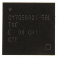
CY7C68001-56LTXC Cypress Semiconductor Corp, CY7C68001-56LTXC Datasheet - Page 41

CY7C68001-56LTXC
Manufacturer Part Number
CY7C68001-56LTXC
Description
IC USB EZ-USB SX2 HS 56VQFN
Manufacturer
Cypress Semiconductor Corp
Series
CY7Cr
Type
USBr
Specifications of CY7C68001-56LTXC
Protocol
USB 2.0
Voltage - Supply
3 V ~ 3.6 V
Mounting Type
Surface Mount
Package / Case
56-VQFN Exposed Pad, 56-HVQFN, 56-SQFN, 56-DHVQFN
Lead Free Status / RoHS Status
Lead free / RoHS Compliant
Number Of Drivers/receivers
-
Lead Free Status / Rohs Status
Lead free / RoHS Compliant
Other names
428-2932
Available stocks
Company
Part Number
Manufacturer
Quantity
Price
Part Number:
CY7C68001-56LTXC
Manufacturer:
CYPRESS/赛普拉斯
Quantity:
20 000
The above sequence diagrams show the timing relation between various SLAVE FIFO signals while performing a read from the
FIFO in synchronous mode where the IFCLK is the clock source. The diagram shows a single read followed by a burst read.
For a burst read the SLRD and SLOE is left asserted during the entire duration of read of all the required bytes. In this burst read
mode, when the SLOE is asserted the data output is the one that the FIFO pointer is pointing to. In this case after the first single
read the FIFO pointer now points to N+1. After the SLRD is asserted, the FIFO pointer is incremented on the immediate rising
edge of the IFCLK when the prefetched data is also output on the data bus. The FIFO pointer is incremented on each subsequent
rising edge of the IFCLK while the SLRD is in an asserted state.
11.6.2
The above sequence diagram shows the timing relation between various signals while performing a write to the FIFO in
synchronous mode where the IFCLK is the clock source. The diagram shows a single write followed by burst write of 3 bytes and
committing the 4 bytes short packet using the PKTEND pin.
Document #: 38-08013 Rev. *B
PKTEND
FLAGS
FIFOADR
• At t = 0 the FIFO address is set. Note that t
• Then the SLOE is asserted. This causes the data lines to be in a driven state with the data that the FIFO pointer is currently
• The SLRD and SLCS is then asserted at the same time. The SLRD must meet the setup time of t
• The FIFO pointer is updated on each rising edge of the IFCLK while the SLRD is in an asserted state. This data pointed to by
• At t = 0 the FIFO address is set. Note that t
• Data is then written to the data bus t
• SLWR and SLCS are asserted at the same time. The SLWR must meet the setup time of t
IFCLK
SLWR/
SLCS
SLCS
DATA
prior to a read.
pointing to. In this case of the above example it is the first byte in the FIFO. Note that the data is pre-fetched and is output only
when the SLOE is asserted. SLOE is an output enable only. It has no other functions besides enabling the data bus to be in
a driven state.
the clock and must maintain the hold time of t
asserted state when SLRD is also asserted. When SLCS is used, the internal logic basically ANDs these two signal to determine
a valid condition. Hence these signals can also be tied together.
the updated FIFO pointer is than output after a propagation delay of t
diagram data N is the first byte read from the FIFO. When the SLRD is asserted, in order to have the data output on the FIFO
data bus, the SLOE MUST be in an asserted state also. The SLRD and SLOE can also be tied together.
prior to a read.
and must maintain the hold time of t
Single and Burst Synchronous Write
t=0
Figure 11-17. Slave FIFO Synchronous Write Sequence and Timing Diagram
t
SFA
t
t
SFD
SWR
t
N
IFCLK
t
FDH
WRH
SFD
t
WRH
t
XFLG
before the rising edge of the IFCLK to meet the data setup time.
measured from the rising edge of IFCLK. If SLCS is used then, SLCS must be in an
SFA
SFA
RDH
being 25 ns implies that the FIFO address lines need to be set up a clock cycle
being 25 ns implies that the FIFO address lines need to be set up a clock cycle
from the rising edge of IFCLK. If SLCS is used then, SLCS must be in an
>= t
t
SFD
SWR
N+1
t
FDH
t
XFD
SFD
N+2
from the rising edge of the IFCLK. So in the above
t
FDH
t
SFD
t
N+3
SPE
>= t
t
SWR
FDH
t
WRH
PEH
from the rising edge of the clock
t
SRD
FAH
[8]
t
from the rising edge of
XFLG
CY7C68001
Page 41 of 50


