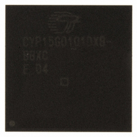
CYP15G0101DXB-BBXC Cypress Semiconductor Corp, CYP15G0101DXB-BBXC Datasheet - Page 19

CYP15G0101DXB-BBXC
Manufacturer Part Number
CYP15G0101DXB-BBXC
Description
IC TXRX HOTLINK 100-LBGA
Manufacturer
Cypress Semiconductor Corp
Series
HOTlink II™r
Type
Transceiverr
Specifications of CYP15G0101DXB-BBXC
Package / Case
100-LBGA
Protocol
Fibre Channel
Voltage - Supply
3.135 V ~ 3.465 V
Mounting Type
Surface Mount
Product
PHY
Data Rate
1500 MBd
Supply Voltage (max)
3.465 V
Supply Voltage (min)
3.135 V
Supply Current
0.5 A
Maximum Operating Temperature
+ 70 C
Minimum Operating Temperature
0 C
Mounting Style
SMD/SMT
Number Of Channels
1
Lead Free Status / RoHS Status
Lead free / RoHS Compliant
For Use With
CYP15G0101DX-EVAL - EVAL BRD FOR HOTLINK II
Number Of Drivers/receivers
-
Lead Free Status / Rohs Status
Lead free / RoHS Compliant
Other names
428-2920
CYP15G0101DXB-BBXC
CYP15G0101DXB-BBXC
Available stocks
Company
Part Number
Manufacturer
Quantity
Price
Company:
Part Number:
CYP15G0101DXB-BBXC
Manufacturer:
MURATA
Quantity:
260 000
Company:
Part Number:
CYP15G0101DXB-BBXC
Manufacturer:
CYPRESS
Quantity:
206
Company:
Part Number:
CYP15G0101DXB-BBXC
Manufacturer:
Cypress Semiconductor Corp
Quantity:
10 000
Part Number:
CYP15G0101DXB-BBXC
Manufacturer:
CYPRESS/赛普拉斯
Quantity:
20 000
Document #: 38-02031 Rev. *J
Receive Modes
The operating mode of the receive path is set through the
RXMODE input. The ‘Reserved for test’ setting (RXMODE =
M) is not allowed, even if the receiver is not being used, as it
will stop normal function of the device. When the decoder is
disabled, the RXMODE setting is ignored as long as it is not a
test mode. These modes determine the RXST status
reporting. The different receive modes are listed in Table 12.
Table 12. Receive Operating Modes
Power Control
The CYP(V)(W)15G0101DXB supports user control of the
powered up or down state of the Transmit and Receive
channel. The Receive channel is controlled by the RXLE
signal and the values present on the BOE[1:0] bus.
The Transmit channel is controlled by the OELE signal and the
values present on the BOE[1:0] bus. If either the Transmit or
the Receive channel is not used, then powering down the
unused channel will save power and reduce system heat
generation. Controlling system power dissipation will improve
the system performance.
Receive Channel
When RXLE = HIGH, the signal on the BOE[0] input directly
controls the power enable for the receive PLL and the analog
circuit. When BOE[0] = HIGH, the Receive channel and its
analog circuits are active. When BOE[0] = LOW, the Receive
channel and its analog circuits are powered down. When
RXLE returns LOW, the values present on the BOE[1:0] inputs
are latched in the Receive Channel Enable Latch. When a
disabled receive channel is re-enabled, the status of the LFI
output and data on the parallel outputs for the Receive channel
may be indeterminate for up to 2 ms.
Transmit Channel
When OELE = HIGH, the signals on the BOE[1:0] inputs
directly control the power enables for the Serial Drivers. When
a BOE[1:0] input is HIGH, the associated Serial Driver is
enabled. When a BOE[1:0] input is LOW, the associated Serial
Driver is disabled. When both Serial Drivers are powered
down, the logic in the entire transmit channel is also powered
down. When OELE returns LOW, the values present on the
BOE[1:0] inputs are latched in the Output Enable Latch.
Device Reset State
When the CYP(V)(W)15G0101DXB is reset by assertion of
TRSTZ, both the Transmit Enable and Receive Enable
Latches are cleared, and the BIST Enable Latch is preset. In
this state, the Transmit and Receive channels are disabled,
and BIST is disabled.
Following a device reset, it is necessary to enable the transmit
and receive channels for normal operation. This can be done
Note:
15. The RXOP output is also driven from the Output Register, but its interpretation is under the separate control of PARCTL.
Number
Mode
0
1
2
RX Mode
RXMODE
M
H
L
Status A
Reserved for test
Status B
RXST Status Reporting
by sequencing the appropriate values on the BOE[1:0] inputs
while the OELE and RXLE signals are raised and lowered. For
systems that do not require dynamic control of power, or want
the part to power up in a fixed configuration, it is also possible
to strap the RXLE and OELE control signals HIGH to perma-
nently enable their associated latches. Connection of the
associated BOE[1:0] signals to a stable HIGH will then enable
the Transmit and Receive channels as soon as the TRSTZ
signal is deasserted.
Output Bus
The receive channel presents a 12-signal output bus
consisting of
The bit assignments of the Data and Status are dependent on
the setting of DECMODE. This mapping is shown in Table 13.
Table 13. Output Register Bit Assignments
When the 10B/8B Decoder is bypassed (DECMODE = LOW),
the framed 10-bit character is presented to the receiver Output
Register, along with a status output (COMDET) indicating if the
character in the Output Register is one of the selected framing
characters. The bit usage and mapping of the external signals
to the raw 10B transmission character is shown in Table 14.
Table 14. Decoder Bypass Mode (DECMODE = LOW)
• an eight-bit data bus
• a three-bit status bus
• a parity bit.
Signal Name
RXST[2]
RXD[7]
RXST[2]
Signal Name
RXD[7]
RXST[1]
RXST[0]
RXD[0]
RXD[1]
RXD[2]
RXD[3]
RXD[4]
RXD[5]
RXD[6]
RXST[1]
RXST[0]
RXD[0]
RXD[1]
RXD[2]
RXD[3]
RXD[4]
RXD[5]
RXD[6]
(MSB)
(LSB)
(MSB)
(LSB)
DECMODE = LOW
COMDET
Bus Weight
DOUT[0]
DOUT[1]
DOUT[2]
DOUT[3]
DOUT[4]
DOUT[5]
DOUT[6]
DOUT[7]
DOUT[8]
DOUT[9]
COMDET
2
2
2
2
2
2
2
2
2
2
CYW15G0101DXB
CYV15G0101DXB
0
1
2
3
4
5
6
7
8
9
CYP15G0101DXB
DECMODE = MID
10B Name
[15]
or HIGH
RXST[2]
RXST[1]
RXST[0]
Page 19 of 39
RXD[0]
RXD[1]
RXD[2]
RXD[3]
RXD[4]
RXD[5]
RXD[6]
RXD[7]
a
b
c
d
e
g
h
i
f
j
[+] Feedback


