ST7540TR STMicroelectronics, ST7540TR Datasheet - Page 38
ST7540TR
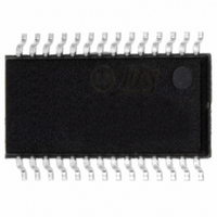
Manufacturer Part Number
ST7540TR
Description
IC TXRX FSK POWER LINE 28-TSSOP
Manufacturer
STMicroelectronics
Type
Transceiverr
Datasheet
1.ST7540TR.pdf
(44 pages)
Specifications of ST7540TR
Number Of Drivers/receivers
1/1
Voltage - Supply
5 V ~ 9 V
Mounting Type
Surface Mount
Package / Case
28-TSSOP Exposed Pad, 28-eTSSOP, 28-HTSSOP
For Use With
497-5485 - BOARD EVAL ST7540 PWR LINE TXRX
Lead Free Status / RoHS Status
Lead free / RoHS Compliant
Protocol
-
Lead Free Status / Rohs Status
Compliant
Other names
497-5528-2
Available stocks
Company
Part Number
Manufacturer
Quantity
Price
Company:

Part Number:
ST7540TR
Manufacturer:
FENGHUA
Quantity:
400 000
Company:
Part Number:
ST7540TR
Manufacturer:
ST
Quantity:
2 100
Part Number:
ST7540TR
Manufacturer:
ST
Quantity:
20 000


Auxiliary analog and digital functions
7.7
7.8
7.9
7.10
7.11
38/44
Under voltage lock out
The UVLO function turns off the device if the V
340mV typically.
Thermal shutdown
The ST7540 is provided of a thermal protection which turn off the PLI when the junction
temperature exceeds 170°C ±10% . Hysteresis is around 30°C.
When shutdown threshold is overcome, PLI interface is switched OFF.
Thermal Shutdown event is notified to the HOST controller using BU/THERM line. When
BU/THERM line is High, ST7540 junction temperature exceed the shutdown threshold (Not
Latched). This function is enabled only in Transmission mode (in Receiving mode the
BU/THERM pin is used for Band in Use signaling, see Band in Use function
Band in
5V Voltage regulator
ST7540 has an embedded 5V linear regulator externally available (on pin VDC) to supply
the application circuitry. The 5V linear regulator has a very low quiescent current (50µA) and
a current capability of 50mA. The regulator is protected against short circuitry events.
3.3V Voltage regulator
The V
pin is externally forced to 5V all the Digital I/Os operate at 5V, otherwise all the Digital I/Os
are internally supplied at 3.3V. The V
components. The 3.3V linear regulator has a very low quiescent current (50µA) and a
current capability of 50mA. The regulator is protected against short circuitry events.
Power-up procedure
To ensure ST7540 proper power-Up sequence, V
following rules:
1.
2.
When V
can be ignored if VDC load < 50mA and if the filtering capacitor on VDC < 100uF.
If V
50mA and the filtering capacitor on V
DD
V
When V
DD
CC
is not forced to 5V, the Digital I/Os are internally supplied at 3.3 V and if V
DD
use).
pin can act either as 3.3V Voltage Output or as Input Digital Supply. When the V
rising slope must not exceed 100V/ms.
supply is connected to VDC (5V Digital Supply) the above mentioned relation
DD
is below 5V/3.3V: V
CC
DD
DD
-V
pin can also source 3.3V voltage to supply external
< 100uF the second relation can be ignored .
DD
< 1.2V.
CC
CC
voltage falls under 4V. Hysteresis is
and V
DD
Supply has to fulfil the
Section 7.1:
DD
load <
ST7540
DD
Related parts for ST7540TR
Image
Part Number
Description
Manufacturer
Datasheet
Request
R

Part Number:
Description:
IC TXRX FSK POWER LINE 28-TSSOP
Manufacturer:
STMicroelectronics
Datasheet:

Part Number:
Description:
STMicroelectronics [RIPPLE-CARRY BINARY COUNTER/DIVIDERS]
Manufacturer:
STMicroelectronics
Datasheet:
Part Number:
Description:
STMicroelectronics [LIQUID-CRYSTAL DISPLAY DRIVERS]
Manufacturer:
STMicroelectronics
Datasheet:

Part Number:
Description:
BOARD EVAL FOR MEMS SENSORS
Manufacturer:
STMicroelectronics
Datasheet:
Part Number:
Description:
NPN TRANSISTOR POWER MODULE
Manufacturer:
STMicroelectronics
Datasheet:
Part Number:
Description:
TURBOSWITCH ULTRA-FAST HIGH VOLTAGE DIODE
Manufacturer:
STMicroelectronics
Datasheet:
Part Number:
Description:
Manufacturer:
STMicroelectronics
Datasheet:
Part Number:
Description:
DIODE / SCR MODULE
Manufacturer:
STMicroelectronics
Datasheet:
Part Number:
Description:
DIODE / SCR MODULE
Manufacturer:
STMicroelectronics
Datasheet:
Part Number:
Description:
Search -----> STE16N100
Manufacturer:
STMicroelectronics
Datasheet:
Part Number:
Description:
Search ---> STE53NA50
Manufacturer:
STMicroelectronics
Datasheet:
Part Number:
Description:
NPN Transistor Power Module
Manufacturer:
STMicroelectronics
Datasheet: