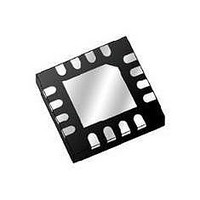
MD1812K6-G Supertex, MD1812K6-G Datasheet - Page 3

MD1812K6-G
Manufacturer Part Number
MD1812K6-G
Description
MOSFET & Power Driver ICs High Speed Quad
Manufacturer
Supertex
Type
High Side/Low Sider
Datasheet
1.MD1812K6-G.pdf
(6 pages)
Specifications of MD1812K6-G
Rise Time
6 ns
Fall Time
6 ns
Supply Voltage (min)
4.5 V
Supply Current
7 mA
Maximum Power Dissipation
2200 mW
Maximum Operating Temperature
+ 125 C
Mounting Style
SMD/SMT
Package / Case
QFN-16
Number Of Drivers
4
Number Of Outputs
4
Lead Free Status / Rohs Status
Lead free / RoHS Compliant
DC Electrical Characteristics
(V
AC Electrical Characteristics
(V
Outputs
(V
l t
H
H
H
R
R
I
l t
t
SOURCE
= V
= V
= V
R
R
PLH
Sym
t
Sym
SOURCE
SOURCE
Sym
OE_OFF
I
OE_ON
∆t
t
R
C
t
SINK
V
V
t
V
V
r
SINK
SINK
I
PCG
I
PLH
PHL
t
t
t
IH
- t
IL
irf
-t
DD
IH
IH
IN
IN
DD
DD
IL
IL
r
f
dm
PHL
f
= 12V, V
= 12V, V
= 12V, V
l
l
Output sink resistance for OUTA-D
Output source resistance for OUTA-D
Output sink resistance for for OUTG
Output source resistance for OUTG
Peak output sink current
Peak output source current
Parameter
Parameter
Input logic voltage high
Input logic voltage low
Input logic current high
Input logic current low
OE Input logic voltage high
OE Input logic voltage low
Input logic impedance to GND
Logic input capacitance
Supertex inc.
Parameter
Input or OE rise & fall time
Propagation delay when output is
from low to high for OUTA-D
Propagation delay when output is
from high to low for OUTA-D
Propagation delay INC to OUTG*
Output rise time for OUTA-D
Output fall time
Rise and fall time matching
Propagation low to high and high to
low matching
Propagation delay matching
Output enable time
L
L
L
= V
= V
= V
SS
SS
SS
= GND = 0V, V
= GND = 0V, V
= GND = 0V, V
NEG
NEG
NEG
●
= -6.0V, V
= -6.0V, V
= -6.0V, V
1235 Bordeaux Drive, Sunnyvale, CA 94089
OE
OE
OE
(cont.)
= 3.3V, T
= 3.3V, T
= 3.3V, T
V
J
J
J
OE
Min
= 25
= 25
= 25
Min
1.7
Min
10
0
0
-
-
-
-
-
-
-
-
-
-0.3
-
-
-
-
-
-
-
-
-
-
-
O
O
O
C)
C)
C)
±2.0
3
Typ
Typ
200
7.0
7.0
6.0
6.0
1.0
1.0
9.0
2.0
2.0
40
Typ
5.0
-
-
-
-
-
20
-
-
-
-
-
-
Max
Max
12.5
12.5
200
200
10
-
-
-
-
-
-
-
-
-
-
-
-
Max
5.0
0.3
1.0
1.0
5.0
0.3
30
10
●
Units
Units
Tel: 408-222-8888
ns
ns
ns
ns
ns
ns
Ω
Ω
Ω
Ω
A
A
Units
KΩ
µA
pF
V
V
Conditions
Conditions
Logic input edge speed requirement
C
Input signal rise/fall time 2ns
* No load
for each channel
Device to device delay match
---
I
I
I
I
---
---
SINK
SOURCE
SINK
SOURCE
LOAD
Conditions
For logic inputs INA, INB, INC, and
IND
For logic input OE
---
= 50mA
= 5.0mA
= 1000pF, see timing diagram
= 50mA
= 5.0mA
●
www.supertex.com


