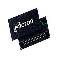
MT46V64M8BN-6:FTR Micron Technology Inc, MT46V64M8BN-6:FTR Datasheet - Page 76

MT46V64M8BN-6:FTR
Manufacturer Part Number
MT46V64M8BN-6:FTR
Description
Manufacturer
Micron Technology Inc
Datasheet
1.MT46V64M8BN-6FTR.pdf
(91 pages)
Specifications of MT46V64M8BN-6:FTR
Lead Free Status / Rohs Status
Compliant
- Current page: 76 of 91
- Download datasheet (4Mb)
Figure 40:
Figure 41:
PDF: 09005aef80a1d9d4/Source: 09005aef82a95a3a
DDR_x4x8x16_Core2.fm - 512Mb DDR: Rev. N; Core DDR Rev. B 2/09 EN
Nonconsecutive WRITE-to-WRITE
Random WRITE Cycles
Notes:
Notes:
t DQSS (NOM)
1. DI b (or n) = data-in from column b (or column n).
2. Three subsequent elements of data-in are applied in the programmed order following DI b.
3. Three subsequent elements of data-in are applied in the programmed order following DI n.
4. An uninterrupted burst of 4 is shown.
5. Each WRITE command may be to any bank.
Command
1. DI b (or x or n or a or g) = data-in from column b (or column x, or column n, or column a, or
2. b', x', n', a' or g' indicate the next data-in following DO b, DO x, DO n, DO a, or DO g,
3. Programmed BL = 2, BL = 4, or BL = 8 in cases shown.
4. Each WRITE command may be to any bank.
Address
Command
column g).
respectively.
Address
DQS
CK#
DM
DQ
CK
DQS
CK#
DM
DQ
CK
WRITE
Bank,
Col b
T0
WRITE
Bank,
Col b
T0
t DQSS (NOM)
t DQSS
WRITE
Bank,
Col x
DI
T1
b
NOP
DI
T1
b
76
T1n
DI
b'
T1n
WRITE
Bank,
Col n
Micron Technology, Inc., reserves the right to change products or specifications without notice.
T2
DI
x
NOP
T2
T2n
DI
x'
512Mb: x4, x8, x16 DDR SDRAM
T2n
WRITE
Bank,
Col a
T3
DI
n
WRITE
Bank,
Col n
T3
Transitioning Data
T3n
DI
n'
Transitioning Data
©2000 Micron Technology, Inc. All rights reserved.
WRITE
Bank,
Col g
T4
DI
a
NOP
DI
T4
n
T4n
DI
a'
T4n
Operations
NOP
T5
DI
g
Don’t Care
T5
NOP
Don’t Care
T5n
DI
g'
T5n
Related parts for MT46V64M8BN-6:FTR
Image
Part Number
Description
Manufacturer
Datasheet
Request
R

Part Number:
Description:
IC SDRAM 64MBIT 133MHZ 54TSOP
Manufacturer:
Micron Technology Inc
Datasheet:

Part Number:
Description:
IC SDRAM 64MBIT 5.5NS 86TSOP
Manufacturer:
Micron Technology Inc
Datasheet:

Part Number:
Description:
IC SDRAM 64MBIT 200MHZ 86TSOP
Manufacturer:
Micron Technology Inc
Datasheet:

Part Number:
Description:
IC SDRAM 64MBIT 133MHZ 54TSOP
Manufacturer:
Micron Technology Inc
Datasheet:

Part Number:
Description:
IC SDRAM 128MBIT 133MHZ 54TSOP
Manufacturer:
Micron Technology Inc
Datasheet:

Part Number:
Description:
IC SDRAM 256MBIT 133MHZ 90VFBGA
Manufacturer:
Micron Technology Inc
Datasheet:

Part Number:
Description:
IC SDRAM 128MBIT 133MHZ 54TSOP
Manufacturer:
Micron Technology Inc
Datasheet:

Part Number:
Description:
IC SDRAM 256MBIT 133MHZ 54TSOP
Manufacturer:
Micron Technology Inc
Datasheet:

Part Number:
Description:
IC DDR SDRAM 512MBIT 6NS 66TSOP
Manufacturer:
Micron Technology Inc
Datasheet:

Part Number:
Description:
IC SDRAM 128MBIT 167MHZ 86TSOP
Manufacturer:
Micron Technology Inc
Datasheet:

Part Number:
Description:
IC SDRAM 128MBIT 143MHZ 86TSOP
Manufacturer:
Micron Technology Inc
Datasheet:

Part Number:
Description:
SDRAM 256M-BIT 1.8V 54-PIN VFBGA
Manufacturer:
Micron Technology Inc
Datasheet:

Part Number:
Description:
IC SDRAM 128MBIT 143MHZ 86TSOP
Manufacturer:
Micron Technology Inc
Datasheet:

Part Number:
Description:
IC SDRAM 128MBIT 125MHZ 54VFBGA
Manufacturer:
Micron Technology Inc
Datasheet:

Part Number:
Description:
IC SDRAM 128MBIT 125MHZ 54VFBGA
Manufacturer:
Micron Technology Inc
Datasheet:


