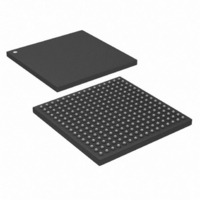
DS26528G+ Maxim Integrated Products, DS26528G+ Datasheet - Page 148

DS26528G+
Manufacturer Part Number
DS26528G+
Description
IC TXRX T1/E1/J1 OCT 256-CSBGA
Manufacturer
Maxim Integrated Products
Type
Transceiverr
Datasheet
1.DS26528G.pdf
(276 pages)
Specifications of DS26528G+
Number Of Drivers/receivers
4/4
Protocol
IEEE 1149.1
Voltage - Supply
3.135 V ~ 3.465 V
Mounting Type
Surface Mount
Package / Case
256-CSBGA
Lead Free Status / RoHS Status
Lead free / RoHS Compliant
- Current page: 148 of 276
- Download datasheet (2Mb)
Register Name:
Register Description:
Register Address:
Bit #
Name
Default
Bit 7: Input Data Format (IDF).
Bit 5: RSER Control (RSERC).
Bit 1: Payload Loopback (PLB).
When PLB is enabled, the following will occur:
In a PLB situation, the DS26528 loops the 192 bits (248 for E1) of payload data (with BPVs corrected) from the
receive section back to the transmit section. The transmitter follows the frame alignment provided by the receiver.
The receive frame boundary is automatically fed into the transmit section, such that the transmit frame position is
locked to the receiver (i.e., TSYNC is sourced from RSYNC). The FPS framing pattern, CRC-6 calculation, and the
FDL bits (FAS word, Si, Sa, E-bits, and CRC-4 for E1) are not looped back. Rather, they are reinserted by the
DS26528 (i.e., the transmit section will modify the payload as if it was input at TSER).
Bit 0: Framer Loopback (FLB).
This loopback is useful in testing and debugging applications. In FLB, the DS26528 loops data from the transmit
side back to the receive side. When FLB is enabled, the following will occur:
1) Data will be transmitted from the TTIP and TRING pins synchronous with RCLK instead of TCLK.
2) All the receive-side signals will continue to operate normally.
3) The TCHCLK and TCHBLK signals are forced low.
4) Data at the TSER, TDATA, and TSIG pins is ignored.
5) The TLCLK signal will become synchronous with RCLK instead of TCLK.
1) (T1 mode) An unframed all-ones code will be transmitted at TTIP and TRING.
2) Data at RTIP and RRING will be ignored.
3) All receive-side signals will take on timing synchronous with TCLK instead of RCLK.
4) Note that it is not acceptable to have RCLK tied to TCLK during this loopback because this will cause an
0 = bipolar data is expected at RTIP and RRING (either AMI or B8ZS)
1 = NRZ data is expected at RTIP. The BPV counter will be disabled and RRING will be ignored by the
DS26528.
0 = allow RSER to output data as received under all conditions (normal operation)
1 = force RSER to one under loss of frame alignment conditions
0 = loopback disabled
1 = loopback enabled
0 = loopback disabled
1 = loopback enabled
(E1 mode) Normal data will be transmitted at TTIP and TRING.
unstable condition.
IDF
7
0
RCR3
Receive Control Register 3
083h + (200h x n): where n = 0 to 7, for Ports 1 to 8
—
6
0
RSERC
5
0
148 of 276
—
4
0
—
3
0
DS26528 Octal T1/E1/J1 Transceiver
—
2
0
PLB
1
0
FLB
0
0
Related parts for DS26528G+
Image
Part Number
Description
Manufacturer
Datasheet
Request
R

Part Number:
Description:
MAX7528KCWPMaxim Integrated Products [CMOS Dual 8-Bit Buffered Multiplying DACs]
Manufacturer:
Maxim Integrated Products
Datasheet:

Part Number:
Description:
Single +5V, fully integrated, 1.25Gbps laser diode driver.
Manufacturer:
Maxim Integrated Products
Datasheet:

Part Number:
Description:
Single +5V, fully integrated, 155Mbps laser diode driver.
Manufacturer:
Maxim Integrated Products
Datasheet:

Part Number:
Description:
VRD11/VRD10, K8 Rev F 2/3/4-Phase PWM Controllers with Integrated Dual MOSFET Drivers
Manufacturer:
Maxim Integrated Products
Datasheet:

Part Number:
Description:
Highly Integrated Level 2 SMBus Battery Chargers
Manufacturer:
Maxim Integrated Products
Datasheet:

Part Number:
Description:
Current Monitor and Accumulator with Integrated Sense Resistor; ; Temperature Range: -40°C to +85°C
Manufacturer:
Maxim Integrated Products

Part Number:
Description:
TSSOP 14/A�/RS-485 Transceivers with Integrated 100O/120O Termination Resis
Manufacturer:
Maxim Integrated Products

Part Number:
Description:
TSSOP 14/A�/RS-485 Transceivers with Integrated 100O/120O Termination Resis
Manufacturer:
Maxim Integrated Products

Part Number:
Description:
QFN 16/A�/AC-DC and DC-DC Peak-Current-Mode Converters with Integrated Step
Manufacturer:
Maxim Integrated Products

Part Number:
Description:
TDFN/A/65V, 1A, 600KHZ, SYNCHRONOUS STEP-DOWN REGULATOR WITH INTEGRATED SWI
Manufacturer:
Maxim Integrated Products

Part Number:
Description:
Integrated Temperature Controller f
Manufacturer:
Maxim Integrated Products

Part Number:
Description:
SOT23-6/I�/45MHz to 650MHz, Integrated IF VCOs with Differential Output
Manufacturer:
Maxim Integrated Products

Part Number:
Description:
SOT23-6/I�/45MHz to 650MHz, Integrated IF VCOs with Differential Output
Manufacturer:
Maxim Integrated Products

Part Number:
Description:
EVALUATION KIT/2.4GHZ TO 2.5GHZ 802.11G/B RF TRANSCEIVER WITH INTEGRATED PA
Manufacturer:
Maxim Integrated Products

Part Number:
Description:
QFN/E/DUAL PCIE/SATA HIGH SPEED SWITCH WITH INTEGRATED BIAS RESISTOR
Manufacturer:
Maxim Integrated Products
Datasheet:


