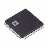
ADV7184BSTZ Analog Devices Inc, ADV7184BSTZ Datasheet - Page 7

ADV7184BSTZ
Manufacturer Part Number
ADV7184BSTZ
Description
IC DECODER VID SDTV MULTI 80LQFP
Manufacturer
Analog Devices Inc
Type
Video Decoderr
Specifications of ADV7184BSTZ
Applications
Projectors, Recorders, Security
Voltage - Supply, Analog
3.15 V ~ 3.45 V
Voltage - Supply, Digital
1.65 V ~ 2 V
Mounting Type
Surface Mount
Package / Case
80-LQFP
Resolution (bits)
10bit
Adc Sample Rate
54MSPS
Power Dissipation Pd
550mW
No. Of Input Channels
12
Supply Voltage Range
1.65V To 2V, 3V To 3.6V
Operating Temperature Range
-40°C To +85°C
Tv /
RoHS Compliant
Input Format
Analogue
Output Format
Digital
Rohs Compliant
Yes
Lead Free Status / RoHS Status
Lead free / RoHS Compliant
Available stocks
Company
Part Number
Manufacturer
Quantity
Price
Company:
Part Number:
ADV7184BSTZ
Manufacturer:
Analog Devices Inc
Quantity:
10 000
THERMAL SPECIFICATIONS
Table 4.
Parameter
Junction-to-Case Thermal Resistance
Junction-to-Ambient Thermal Resistance (Still Air)
TIMING SPECIFICATIONS
A
otherwise noted).
Table 5.
Parameter
SYSTEM CLOCK AND CRYSTAL
I
RESET FEATURE
CLOCK OUTPUTS
DATA AND CONTROL OUTPUTS
1
2
3
4
2
Temperature range T
Guaranteed by characterization.
TTL input values are 0 V to 3 V, with rise/fall times of ≤3 ns, measured between the 10% and 90% points.
SDP timing figures obtained using default drive strength value (0xD5) in Register 0xF4.
C PORT
VDD
Nominal Frequency
Frequency Stability
SCLK Frequency
SCLK Minimum Pulse Width High
SCLK Minimum Pulse Width Low
Hold Time (Start Condition)
Setup Time (Start Condition)
SDA Setup Time
SCLK and SDA Rise Time
SCLK and SDA Fall Time
Setup Time for Stop Condition
Reset Pulse Width
LLC1 Mark-Space Ratio
LLC1 Rising to LLC2 Rising
LLC1 Rising to LLC2 Falling
Data Output Transitional Time
Data Output Transitional Time
Propagation Delay to High-Z
Max Output Enable Access Time
Min Output Enable Access Time
= 3.15 V to 3.45 V, D
3
1, 2
MIN
to T
MAX
VDD
is −40°C to +85°C. The minimum/maximum specifications are guaranteed over this range.
= 1.65 V to 2.0 V, D
4
4
Symbol
t
t
t
t
t
t
t
t
t
t
t
t
t
t
t
t
1
2
3
4
5
6
7
8
9
11
12
13
14
15
16
17
:t
10
VDDIO
Test Conditions
Negative clock edge to start of valid data
(t
End of valid data to negative clock edge
(t
ACCESS
HOLD
= 3.0 V to 3.6 V, P
= t
Symbol
θ
θ
= t
JC
JA
9
10
+ t
Rev. A | Page 7 of 112
− t
14
)
13
)
Test Conditions
4-layer PCB with solid ground plane
4-layer PCB with solid ground plane
VDD
= 1.71 V to 1.89 V (operating temperature range, unless
Min
0.6
1.3
0.6
0.6
100
5
45:55
Typ
0.6
1
1
6
7
4
28.63636
Min
Max
±50
400
300
300
55:45
Typ
7.6
38.1
3.6
2.4
ADV7184
Unit
ppm
kHz
μs
μs
μs
μs
ns
ns
ns
μs
ms
% duty cycle
ns
ns
ns
ns
ns
ns
ns
Max
MHz
Unit
°C/W
°C/W


