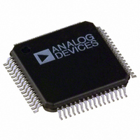
ADV7321KSTZ Analog Devices Inc, ADV7321KSTZ Datasheet - Page 25

ADV7321KSTZ
Manufacturer Part Number
ADV7321KSTZ
Description
IC VID ENC 6-12BIT DAC'S 64LQFP
Manufacturer
Analog Devices Inc
Type
Video Encoderr
Datasheet
1.ADV7321KSTZ.pdf
(88 pages)
Specifications of ADV7321KSTZ
Applications
EVD, DVD, SD/PS/HDTV
Voltage - Supply, Analog
2.5V
Voltage - Supply, Digital
2.5V
Mounting Type
Surface Mount
Package / Case
64-LQFP
Input Format
Digital
Output Format
Analog
Supply Voltage Range
2.375V To 2.625V
Operating Temperature Range
0°C To +70°C
Tv / Video Case Style
LQFP
No. Of Pins
64
Msl
MSL 1 - Unlimited
Lead Free Status / RoHS Status
Lead free / RoHS Compliant
Available stocks
Company
Part Number
Manufacturer
Quantity
Price
Company:
Part Number:
ADV7321KSTZ
Manufacturer:
Micrel
Quantity:
2 023
Company:
Part Number:
ADV7321KSTZ
Manufacturer:
ADI
Quantity:
329
Company:
Part Number:
ADV7321KSTZ
Manufacturer:
Analog Devices Inc
Quantity:
10 000
Part Number:
ADV7321KSTZ
Manufacturer:
ADI/亚德诺
Quantity:
20 000
REGISTER ACCESS
The MPU can write to or read from all registers of the
ADV7320/ADV7321 except the subaddress registers, which are
write only registers. The subaddress register selected determines
which register the next read or write operation will access. All
communication with the part through the bus starts with an
access to the subaddress register. A read/write operation is then
performed from/to the target address, which increments to the
next address until a stop command is performed on the bus.
Table 7. Registers 0x00 to 0x01
SR7–
SR0
0x00
0x01
Register
Power
Mode
Register
Mode
Select
Register
Bit Description
Sleep Mode. With this
control enabled, the
current consumption is
reduced to μA level. All
DACs and the internal
PLL cct are disabled.
I
read from and written
to in sleep mode.
PLL and Oversampling
Control. This control
allows the internal PLL
cct to be powered
down and the
oversampling to be
switched off.
DAC F: Power On/Off.
DAC E: Power On/Off.
DAC D: Power On/Off.
DAC C: Power On/Off.
DAC B: Power On/Off.
DAC A: Power On/Off.
Reserved.
Clock Edge.
Reserved.
Clock Align.
Input Mode.
Y/C/S Bus Swap.
2
C registers can be
Bit 7
0
1
0
1
Bit 6
0
1
0
0
0
0
1
1
1
1
Bit 5
0
1
0
0
1
1
0
0
1
1
Rev. A | Page 25 of 88
Bit 4
1
0
1
0
1
0
1
0
0
1
REGISTER PROGRAMMING
The following tables describe the functionality of each register.
All registers can be read from and written to, unless otherwise
stated.
SUBADDRESS REGISTER (SR7 TO SR0)
Each subaddress register is an 8-bit write only register. After the
encoder’s bus is accessed and a read or write operation is selected,
the subaddress is set up. The subaddress register determines to
or from which register the operation takes place.
Bit 3
0
1
0
1
Bit 2
0
1
0
Bit 1
0
1
0
1
Bit 0
0
1
0
Register Setting
Sleep mode off.
Sleep mode on.
PLL on.
PLL off.
DAC F off.
DAC F on.
DAC E off.
DAC E on.
DAC D off.
DAC D on.
DAC C off.
DAC C on.
DAC B off.
DAC B on.
DAC A off.
DAC A on.
Reserved.
Cb clocked upon
rising edge.
Y clocked upon rising
edge.
Must be set if the
phase delay between
the two input clocks is
<9.25 ns or >27.75 ns.
SD input only.
PS input only.
HDTV input only.
SD and PS (20-bit).
SD and PS (10-bit).
SD and HDTV (SD
oversampled).
SD and HDTV (HDTV
oversampled).
PS only (at 54 MHz).
Allows data to be
applied to data ports
in various
configurations (SD
feature only).
ADV7320/ADV7321
Reset Value
(Shaded)
0xFC
Only for PS
interleaved
input at 27
MHz.
Only if two
input clocks
are used.
0x38
See Table 21.


