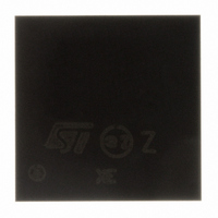
STA015B$ STMicroelectronics, STA015B$ Datasheet - Page 15

STA015B$
Manufacturer Part Number
STA015B$
Description
DECODER AUDIO MPEG 2.5 8X8LFBGA
Manufacturer
STMicroelectronics
Type
Audio Decoderr
Datasheet
1.STA015T.pdf
(56 pages)
Specifications of STA015B$
Applications
Sound Cards, Players, Recorders
Voltage - Supply, Digital
2.4 V ~ 3.6 V
Mounting Type
Surface Mount
Package / Case
64-LFBGA
Lead Free Status / RoHS Status
Lead free / RoHS Compliant
Voltage - Supply, Analog
-
Available stocks
Company
Part Number
Manufacturer
Quantity
Price
Company:
Part Number:
STA015B$13TR
Manufacturer:
STMicroelectronics
Quantity:
10 000
5.1.4 Data input
During the data input the STA015 samples the SDA signal on the rising edge of the clock SCL. For correct
device operation the SDA signal has to be stable during the rising edge of the clock and the data can
change only when the SCL line is low.
5.2 DEVICE ADDRESSING
To start communication between the master and the STA015, the master must initiate with a start condi-
tion. Following this, the master sends onto the SDA line 8 bits (MSB first) corresponding to the device se-
lect address and read or write mode. The 7 most significant bits are the device address identifier,
corresponding to the I
The 8th bit (LSB) is the read or write operation RW, this bit is set to 1 in read mode and 0 for write mode.
After a START condition the STA015 identifies on the bus the device address and, if a match is found, it
acknowledges the identification on SDA bus during the 9th bit time. The following byte after the device
identification byte is the internal space address.
5.3 WRITE OPERATION (see fig. 16)
Following a START condition the master sends a device select code with the RW bit set to 0. The STA015
acknowledges this and waits for the byte of internal address.
After receiving the internal bytes address the STA015 again responds with an acknowledge.
5.3.1 Byte write
In the byte write mode the master sends one data byte, this is acknowledged by STA015. The master then
terminates the transfer by generating a STOP condition.
5.3.2 Multibyte write
The multibyte write mode can start from any internal address. The transfer is terminated by the master
generating a STOP condition.
Figure 16. Write Mode Sequence
Figure 17. Read Mode Sequence
MULTIBYTE
SEQUENTIAL
SEQUENTIAL
WRITE
WRITE
BYTE
CURRENT
ADDRESS
ADDRESS
CURRENT
RANDOM
RANDOM
READ
READ
READ
READ
START
START
START
START
START
START
DEV-ADDR
DEV-ADDR
DEV-ADDR
DEV-ADDR
DEV-ADDR
DEV-ADDR
2
C bus definition. For the STA015 these are fixed as 1000011.
HIGH
RW=
RW
RW
RW
ACK
ACK
ACK
ACK
RW
RW
SUB-ADDR
SUB-ADDR
ACK
ACK
DATA
DATA
NO ACK
ACK
ACK
ACK
SUB-ADDR
SUB-ADDR
START
START
STOP
DATA
DEV-ADDR
DEV-ADDR
ACK
ACK
RW
RW
ACK
ACK
ACK
DATA IN
DATA IN
DATA
DATA
DATA
ACK
ACK
NO ACK
NO ACK
ACK
STOP
STOP
STOP
DATA
D98AU825B
D98AU826A
ACK
DATA IN
DATA
ACK
NO ACK
STA015
STOP
STOP
15/56


