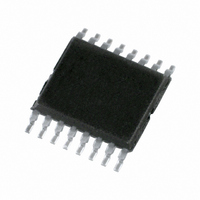
PCA9500PW,112 NXP Semiconductors, PCA9500PW,112 Datasheet - Page 11

PCA9500PW,112
Manufacturer Part Number
PCA9500PW,112
Description
IC I/O EXPANDER I2C 8B 16TSSOP
Manufacturer
NXP Semiconductors
Datasheet
1.PCA9500BS118.pdf
(26 pages)
Specifications of PCA9500PW,112
Package / Case
16-TSSOP
Interface
I²C, SMBus
Number Of I /o
8
Interrupt Output
No
Frequency - Clock
400kHz
Voltage - Supply
2.5 V ~ 3.6 V
Operating Temperature
-40°C ~ 85°C
Mounting Type
Surface Mount
Includes
EEPROM, POR
Logic Family
PCA9500
Number Of Lines (input / Output)
8.0 / 8.0
Operating Supply Voltage
2.5 V to 3.6 V
Power Dissipation
400 mW
Operating Temperature Range
- 40 C to + 85 C
Input Voltage
5 V
Logic Type
I/O Expander
Maximum Clock Frequency
400 KHz
Mounting Style
SMD/SMT
Number Of Input Lines
8.0
Number Of Output Lines
8.0
Output Current
25 mA
Output Voltage
5 V
Operating Temperature (min)
-40C
Operating Temperature Classification
Industrial
Operating Temperature (max)
85C
Package Type
TSSOP
Rad Hardened
No
Lead Free Status / RoHS Status
Lead free / RoHS Compliant
Lead Free Status / RoHS Status
Lead free / RoHS Compliant, Lead free / RoHS Compliant
Other names
568-1025-5
935271534112
PCA9500PW
935271534112
PCA9500PW
NXP Semiconductors
PCA9500_4
Product data sheet
8.2 System configuration
8.3 Acknowledge
A device generating a message is a ‘transmitter’; a device receiving is the ‘receiver’. The
device that controls the message is the ‘master’ and the devices which are controlled by
the master are the ‘slaves’ (see
The number of data bytes transferred between the START and the STOP conditions from
transmitter to receiver is not limited. Each byte of eight bits is followed by one
acknowledge bit. The acknowledge bit is a HIGH level put on the bus by the transmitter,
whereas the master generates an extra acknowledge related clock pulse.
A slave receiver which is addressed must generate an acknowledge after the reception of
each byte. Also a master must generate an acknowledge after the reception of each byte
that has been clocked out of the slave transmitter. The device that acknowledges has to
pull down the SDA line during the acknowledge clock pulse, so that the SDA line is stable
LOW during the HIGH period of the acknowledge related clock pulse; set-up time and hold
time must be taken into account.
A master receiver must signal an end of data to the transmitter by not generating an
acknowledge on the last byte that has been clocked out of the slave. In this event, the
transmitter must leave the data line HIGH to enable the master to generate a STOP
condition.
Fig 17. System configuration
Fig 18. Acknowledgement on the I
SDA
SCL
TRANSMITTER/
RECEIVER
MASTER
SCL from master
by transmitter
data output
by receiver
data output
Rev. 04 — 15 April 2009
condition
START
RECEIVER
SLAVE
S
Figure
8-bit I
2
C-bus
1
2
17).
C-bus and SMBus I/O port with 2-kbit EEPROM
TRANSMITTER/
RECEIVER
SLAVE
2
acknowledgement
not acknowledge
TRANSMITTER
clock pulse for
acknowledge
MASTER
8
PCA9500
© NXP B.V. 2009. All rights reserved.
002aaa987
9
TRANSMITTER/
RECEIVER
MASTER
002aaa381
11 of 26


