PCA9698DGG,512 NXP Semiconductors, PCA9698DGG,512 Datasheet - Page 43
PCA9698DGG,512
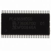
Manufacturer Part Number
PCA9698DGG,512
Description
IC I/O EXPANDER I2C 40B 56TSSOP
Manufacturer
NXP Semiconductors
Datasheet
1.PCA9698BS118.pdf
(48 pages)
Specifications of PCA9698DGG,512
Package / Case
56-TSSOP
Interface
I²C
Number Of I /o
40
Interrupt Output
Yes
Frequency - Clock
1MHz
Voltage - Supply
2.3 V ~ 5.5 V
Operating Temperature
-40°C ~ 85°C
Mounting Type
Surface Mount
Includes
POR
Logic Family
PCA9698
Number Of Lines (input / Output)
40.0 / 40.0
Operating Supply Voltage
2.3 V to 5.5 V
Power Dissipation
500 mW
Operating Temperature Range
- 40 C to + 85 C
Input Voltage
5.5 V
Logic Type
I2C Bus
Maximum Clock Frequency
1 MHz
Mounting Style
SMD/SMT
Number Of Input Lines
40.0
Number Of Output Lines
40.0
Output Current
50 mA
Output Voltage
5.5 V
Lead Free Status / RoHS Status
Lead free / RoHS Compliant
For Use With
OM6281 - DAUGHTER CARD PCA9698 FOR OM6275
Lead Free Status / Rohs Status
Lead free / RoHS Compliant
Other names
568-3241-5
935278614512
PCA9698DGG
935278614512
PCA9698DGG
Available stocks
Company
Part Number
Manufacturer
Quantity
Price

Part Number:
PCA9698DGG,512
Manufacturer:
NXP/恩智浦
Quantity:
20 000


NXP Semiconductors
PCA9698
Product data sheet
16.4 Reflow soldering
Key characteristics in reflow soldering are:
Table 16.
Table 17.
Moisture sensitivity precautions, as indicated on the packing, must be respected at all
times.
Studies have shown that small packages reach higher temperatures during reflow
soldering, see
Package thickness (mm)
< 2.5
≥ 2.5
Package thickness (mm)
< 1.6
1.6 to 2.5
> 2.5
•
•
•
•
•
Process issues, such as application of adhesive and flux, clinching of leads, board
transport, the solder wave parameters, and the time during which components are
exposed to the wave
Solder bath specifications, including temperature and impurities
Lead-free versus SnPb soldering; note that a lead-free reflow process usually leads to
higher minimum peak temperatures (see
reducing the process window
Solder paste printing issues including smearing, release, and adjusting the process
window for a mix of large and small components on one board
Reflow temperature profile; this profile includes preheat, reflow (in which the board is
heated to the peak temperature) and cooling down. It is imperative that the peak
temperature is high enough for the solder to make reliable solder joints (a solder paste
characteristic). In addition, the peak temperature must be low enough that the
packages and/or boards are not damaged. The peak temperature of the package
depends on package thickness and volume and is classified in accordance with
Table 16
SnPb eutectic process (from J-STD-020C)
Lead-free process (from J-STD-020C)
and
Figure
All information provided in this document is subject to legal disclaimers.
17
43.
40-bit Fm+ I
Rev. 3 — 3 August 2010
Package reflow temperature (°C)
Volume (mm
< 350
235
220
Package reflow temperature (°C)
Volume (mm
< 350
260
260
250
2
C-bus advanced I/O port with RESET, OE and INT
3
3
)
)
Figure
350 to 2000
260
250
245
43) than a SnPb process, thus
≥ 350
220
220
245
> 2000
260
245
PCA9698
© NXP B.V. 2010. All rights reserved.
43 of 48
Related parts for PCA9698DGG,512
Image
Part Number
Description
Manufacturer
Datasheet
Request
R

Part Number:
Description:
NXP Semiconductors designed the LPC2420/2460 microcontroller around a 16-bit/32-bitARM7TDMI-S CPU core with real-time debug interfaces that include both JTAG andembedded trace
Manufacturer:
NXP Semiconductors
Datasheet:

Part Number:
Description:
NXP Semiconductors designed the LPC2458 microcontroller around a 16-bit/32-bitARM7TDMI-S CPU core with real-time debug interfaces that include both JTAG andembedded trace
Manufacturer:
NXP Semiconductors
Datasheet:
Part Number:
Description:
NXP Semiconductors designed the LPC2468 microcontroller around a 16-bit/32-bitARM7TDMI-S CPU core with real-time debug interfaces that include both JTAG andembedded trace
Manufacturer:
NXP Semiconductors
Datasheet:
Part Number:
Description:
NXP Semiconductors designed the LPC2470 microcontroller, powered by theARM7TDMI-S core, to be a highly integrated microcontroller for a wide range ofapplications that require advanced communications and high quality graphic displays
Manufacturer:
NXP Semiconductors
Datasheet:
Part Number:
Description:
NXP Semiconductors designed the LPC2478 microcontroller, powered by theARM7TDMI-S core, to be a highly integrated microcontroller for a wide range ofapplications that require advanced communications and high quality graphic displays
Manufacturer:
NXP Semiconductors
Datasheet:
Part Number:
Description:
The Philips Semiconductors XA (eXtended Architecture) family of 16-bit single-chip microcontrollers is powerful enough to easily handle the requirements of high performance embedded applications, yet inexpensive enough to compete in the market for hi
Manufacturer:
NXP Semiconductors
Datasheet:
Part Number:
Description:
The XA-S3 device is a member of Philips Semiconductors? XA(eXtended Architecture) family of high performance 16-bitsingle-chip microcontrollers
Manufacturer:
NXP Semiconductors
Datasheet:

Part Number:
Description:
The NXP BlueStreak LH75401/LH75411 family consists of two low-cost 16/32-bit System-on-Chip (SoC) devices
Manufacturer:
NXP Semiconductors
Datasheet:
Part Number:
Description:
The NXP LPC3130/3131 combine an 180 MHz ARM926EJ-S CPU core, high-speed USB2
Manufacturer:
NXP Semiconductors
Datasheet:
Part Number:
Description:
The NXP LPC3141 combine a 270 MHz ARM926EJ-S CPU core, High-speed USB 2
Manufacturer:
NXP Semiconductors
Part Number:
Description:
The NXP LPC3143 combine a 270 MHz ARM926EJ-S CPU core, High-speed USB 2
Manufacturer:
NXP Semiconductors

Part Number:
Description:
The NXP LPC3152 combines an 180 MHz ARM926EJ-S CPU core, High-speed USB 2
Manufacturer:
NXP Semiconductors
Part Number:
Description:
The NXP LPC3154 combines an 180 MHz ARM926EJ-S CPU core, High-speed USB 2
Manufacturer:
NXP Semiconductors

Part Number:
Description:
Standard level N-channel enhancement mode Field-Effect Transistor (FET) in a plastic package using NXP High-Performance Automotive (HPA) TrenchMOS technology
Manufacturer:
NXP Semiconductors
Datasheet: